


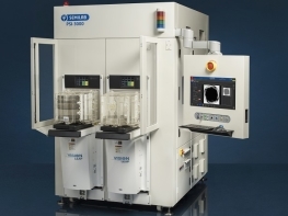
PSI-3000 Polarized Stress Imaging System
The PSI product line is developed for the automated fabs with high capacity and is specialized for the inspection and visualization of crystal defects related to mechanical stress in Si wafers or slugs.
Features and System Specifications:
- SAM2™ (Semilab Automation Manager 2) user interface compliant to SEMI® standard (E95-0200)
- High precision robot for 300 mm wafers with selectable edge-grip or backside contact end effector
- Option: dual side particle detection on surface
| PSI-3000 | |
|---|---|
| Wafer size | 150 mm / 200 mm / 300 mm |
| Loading | Automatic for one selected sample size Manual loading for one or two additional diameters |
| Platform | Dual FOUP load port capability, SECS/GEM and OHT |
Applications:
- Detection of crystal defect related stress fields in as-grown Si wafers or slugs before wafer state.
- Defect types:
- Localized dislocations
- Slip lines
- Twin lines
- Epi process caused edge defects
Request Info