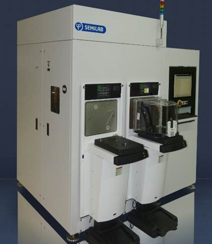
IR-2100, IR-2200, IR-2500, IR-3200
Extended wavelength model-based infrared reflectometry with high throughput, low COO, non-contact, non-destructive measurements of thickness and uniformity of dielectric layers and etched structures used in integrated circuit manufacturing. The unique technology and analysis capability of the IR product line, simplifies system calibration requirements and removes the effect of substrate variations for key layer measurements.
Features and system specifications:
- Product series and sample size:
- IR-2100: Coupon size up to 300 mm
- IR-2200: 150/200 mm, with one open cassette or SMIF loadport
- IR-2500: 300 mm, with one FOUP loadport
- IR-3200: 200/300 mm, with two open cassette, SMIF or FOUP loadports.
- Each product is available with one of the following MBIR optics:
- The large spot optics are mainly used for films or for measurements in the device area of patterned wafers.
- The small spot optics enable measurements of scribe line test structures on patterned wafers.
- Cognex Patmax© pattern recognition
- Camera-based autofocus
- Robust glowbar/halogen source with a lifetime > 3 years
- Conformity:
- EMC directive
- Low voltage directive
- SEMI standards compliant
- Windows-based software with menu-driven recipe selection/generation


