


Application
CONTAMINATION ANALYSIS
Semilab offers various solutions to analyze semiconductor samples. These are all aimed to give as much information on the subject as possible to help people understand the sources of the behavior and properties of their samples and the effects of the used processes.
Using the state-of-the-art Deep Level Transient Spectroscopy (DLTS) setup of the Semilab DLS-1100, it is possible to perform qualitative and quantile analysis of the electrically active impurities and defects in the semiconductor, although this is a destructive technique. This method provides information about the activation energy of the impurity and capture cross section. It also allows to the detection of concentration impurities down to 5×10⁷ atoms/cm3 depending on the doping concentration.
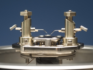 Figure 1. Contamination analysis
Technology
DEEP LEVEL TRANSIENT SPECTROSCOPY
The Deep Level Transient Spectroscopy (DLTS) is a powerful technology for the detection and identification of electrically active defects (known as traps) in semiconductors. These can occur due to contamination or crystal defects. It is an extremely versatile method for determining all parameters associated with deep traps, including energy level, capturing cross section and concentration distribution. It allows the identification of the impurities and is capable of detecting contamination concentrations.
DLTS is a destructive technique, as it requires the forming of either a Schottky-diode, or a p-n junction with a small sample, usually cut from a complete wafer.
The system is composed either of the DLS-83D or DLS-1100 and one of the four cryostats that Semilab offers.
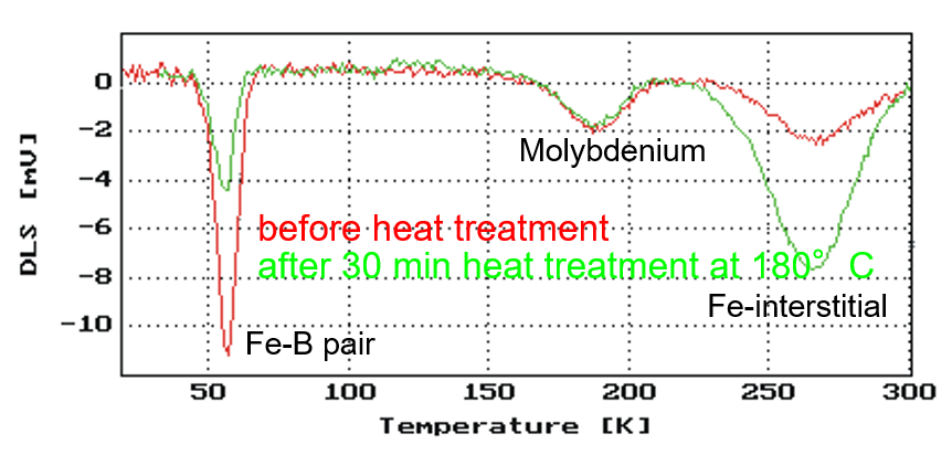 Figure 2. Measurement results
The majority carrier traps are observed by the application of a reverse bias pulse, while the minority carrier traps can be observed by the application of a forward bias pulse.
The technique works by observing the capacitance transient, associated with the change in depletion region width as the diode returns to equilibrium from an initial non-equilibrium state.
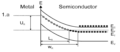
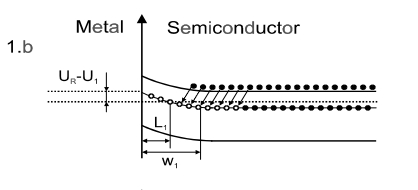
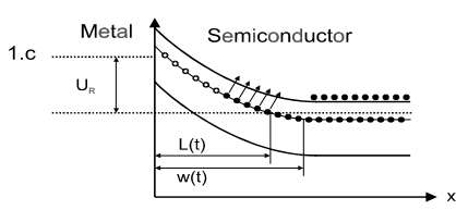
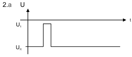
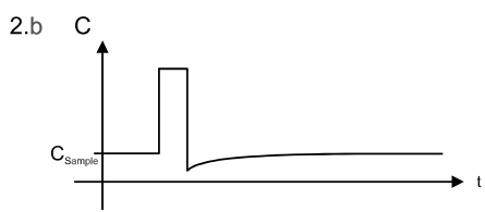
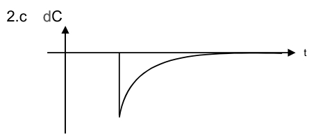
Figure 3. Capacitance transients generated by voltage change
As the emission process is very fast, the capacitance transient is small and noisy. In order to slow down the emission process, different kind of cryostats can be used for cooling the sample (usually in the range from 30 K to room temperature 300 K, or above). The result of the cooling is a longer transient. By using a lock-in averaging technique, peaks at a particular emission rate are detected as a function of temperature. By looking for emissions at different frequencies, and monitoring the temperature of the associated peak, an Arrhenius plot allows the deduction of a trap's activation energy. By varying the pulse width, it is possible to determine the capture cross-section precisely.
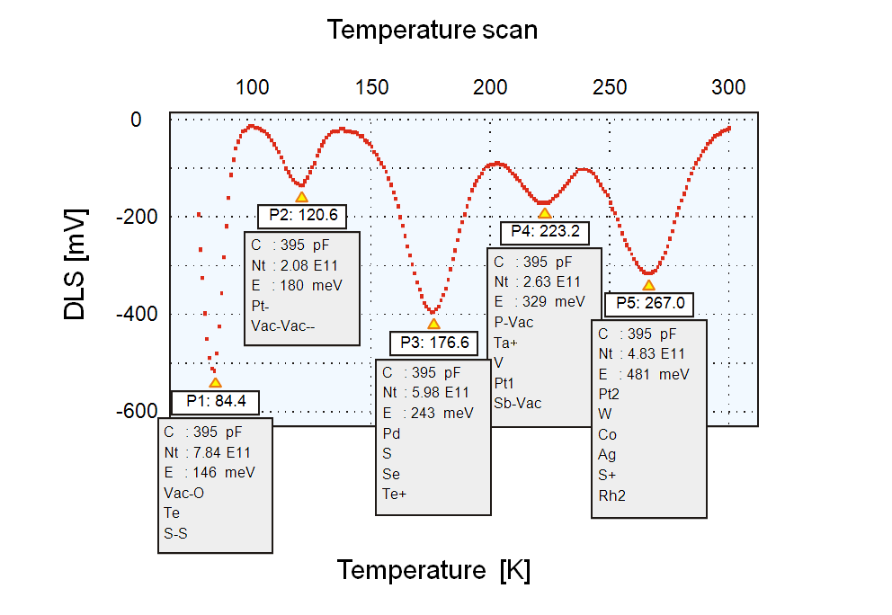
Figure 4. DLTS peak identification
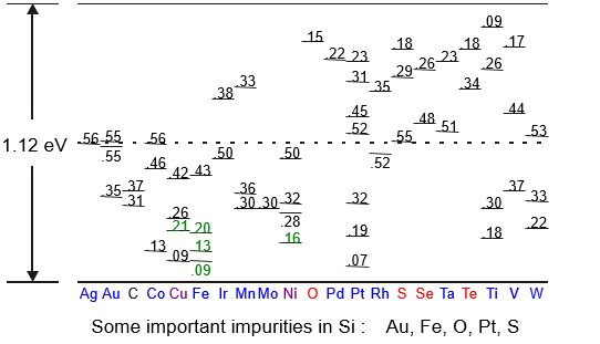
Figure 5. Activation energies for various impurities
ARRHENIUS PLOT LIBRARY:
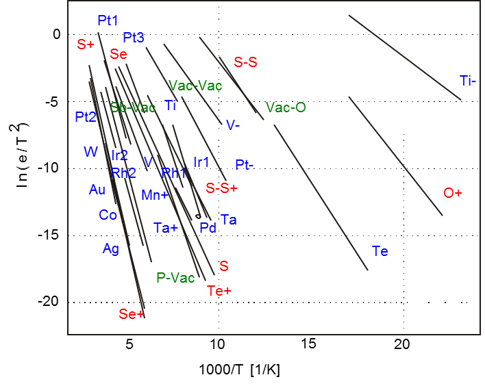 Figure 6. Measurement results
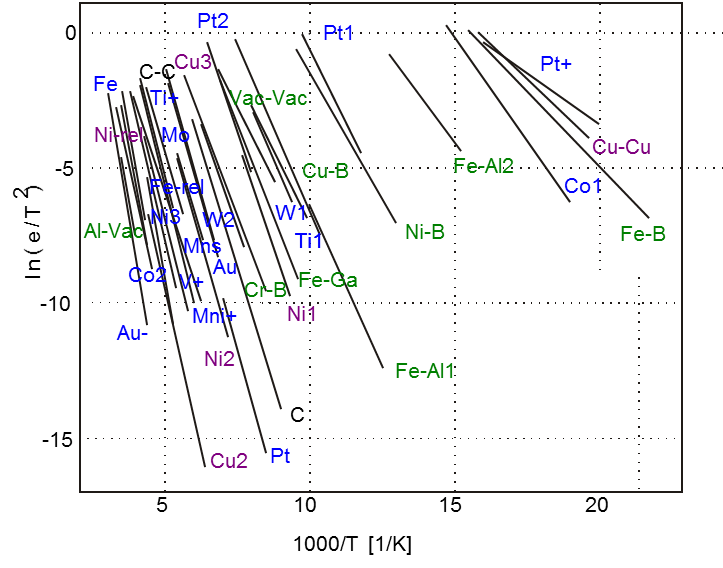 Figure 7. Measurement results
With the help of direct transient recording option it is possible to extract the full Arrhenius plot from a single temperature scan, significantly reducing the sample measurement time.
.jpg) Figure 8. Measurement results
Figure 8. Measurement results
FEATURES
- State-of-the-art contamination identification with the highest sensitivity available on the market
- Complete range of measurement modes, including temperature scan, frequency scan, depth profiling, C-V characterization, capture cross-section measurement, optical injection, conductance transient measurements
- Controlled by user-friendly GUI
-
Sample quality test by I-V and C-V
-
Full computer control with extensive software support featuring the latest evaluation procedures of physics of deep levels, complete (extensive and expandable) library database for accurate contamination determination
- Different cryostats with wide temperature ranges are available, depending on the application requirements
Product Line
DLS
Interfacing to a broad range of cryostats
Complete range of measurement modes:
- Temperature scan
- Frequency scan
- Depth profiling
- C-V characterization
- Capture cross section measurement
- Optical injection
- Conductance transient measurements
Optional digital or analog control of settings to allow real ease of operation
- Sample quality test by I-V, C-V
- Full computer control with extensive software support, complete library database for accurate contamination identification
.jpg)
Products

DLS-83D Deep Level Transient Spectrometer
The DLS-83D offers a fully automatic measurement mode, as well as provides complete interpretation of the measured data, including impurity identification and concentration determination without any need for user interaction.
The Deep Level Transient Spectroscopy (DLTS) is the best technique for monitoring and characterizing deep levels caused by intentionally or unintentionally introduced impurities and defects in semiconductor materials and complete devices. It is an extremely versatile method for determining all parameters associated with deep traps, including energy level, capturing cross section and concentration distribution. It allows the identification of the impurities, and is capable of detecting contamination concentrations below 109 atoms/cm3.
Features and system specifications:
- Highest sensitivity (109 atoms/cm3) for detection of trace levels of contamination
- Interfacing to a broad range of cryostats
- Wide range of measurement modes:
- temperature scan
- frequency scan
- depth profiling
- C-V characterization
- capture cross section measurement
- optical injection
- constant capacitance feedback loop
- conductance transient measurements
- MOS interface state density distribution
- controlled by digital and analog settings to allow real ease of operation
- sample quality test by I-V, C-V
- full computer control with extensive software support, complete library database for accurate contamination identification


Cryostats for Semilab DLS systems
Semilab offers the following Cryostats to use with the DLS systems:
- Low vibration cryostat chamber 30K-400K (optionally up to 800K) – equipped with manipulators for easily establishing good electrical contact on small samples and devices and for readjusting the contact needles at low temperatures still under vacuum.
- Bath type cryostat: 77K-450K –– heating is computer-controlled – controller built into DLS-1000. Convectional (in LN2 atmosphere)
- Automatic LN2 cryostat 80K - 550K (maximum 800K optional). Sample in the vacuum chamber – requires computer-controlled heating and cooling (by LN2 boiling), requires controller and cryostat control unit.
- Automatic He (closed cycle) vacuum cryostat*: 30K - 325K. Controller is commercial LakeShore – controlled by the DLS control software.
*Vacuum cryostats require vacuum pump (not included by default)
Request Info
DLS-1100 Deep Level Transient Spectrometer
DLS-1100 Deep Level Transient Spectrometer provides metrology of the highest sensitivity for characterization and identification of impurities ans defects (known as traps) for the wafermaker market and research institutes.
The new technologies - a low-vibration cryostat with improved signal-to-noise ratio, a more accurate temperature controller and the improved evaluation software - allow for automatic control of the experimental parameters and automatic evaluation of trap concentration, activation energy and capture cross section on semiconductor samples.
Applications and Measurement modes
Electrically active defects’ identification and complete range of measurement modes, including:
- Sample quality test by I-V, C-V
- Capacitance transient measurement by using lock-in integrator for
- temperature scan,
- frequency scan,
- depth profiling,
- capture cross section,
- MOS interface state density distribution measurements
- Digitization of the capacitance transient and evaluation for further analysis via Transient recorder
- Current DLS (I-DLS) option for high conductivity samples
Cryostats
DLS-1100 system can be combined with different cryostats capable of measuring with different temperature ranges:
- Low vibration cryostat chamber 30K-400K (optionally up to 800K)
- Closed Cycle He-cryostat from 30K to 325K
- Bath-type Liquid Nitrogen cryostat (77K – 450K)
- Automatic LN2 cryostat with controlled LN2 flow from 80K to 550K or from 80K to 800K
Benefits
- Highest sensitivity for detection of trace levels of contaminants: down to 5x10⁷ atoms/cm3
- More accurate temperature measurement (<1 K) with up to 10 sensors
- Fully automated measurements, capability of capacitance transient digitization and numerical evaluation due to evaluation software improvements