


Application
DEFECT INSPECTION
“Bulk Micro Defects” (BMD) is a term commonly used to refer to oxygen precipitates in silicon. In fact, many imperfections in the silicon lattice create defects, and BMDs could be any imperfections including oxygen precipitates, voids, inclusions and so on.
BMDs go by many names, referring to the problems they cause, how they were created, or their physical characteristics. Examples include COPs (Crystal Originated Particles) and Grown-In Defects.
Dislocations can be formed during crystal growth, but also at thermal processing of wafers, during CMOS device manufacturing, like epitaxial layer growth and implant anneal steps.
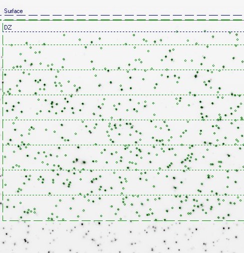 Figure 1. Bulk Micro Defects
Imperfections in the lattice of a semiconductor and impurities create energy states in the bandgap, decrease carrier lifetime, and increase junction leakage. They also act as gettering sites, at which impurities tend to concentrate. The profile of the BMDs is often controlled as shown in Figure 1. by a complex series of high temperature processes to create a “denuded zone”. By this, the surface layer silicon, where the MOS transistor action takes place is free of oxygen precipitates, and the oxygen precipitates in the underlying silicon act as a gettering site to keep impurities away from the MOS transistors.
IR light penetrates most semiconductor materials, and since BMDs alter the local optical properties of a semiconductor, BMDs can be detected by illuminating a sample with IR light and looking at it with a camera that is sensitive to IR.
Technology
EN-VISION
En-Vision (Enhanced Vision) provides non-contact measurements of buried defects, such as dislocations, oxygen precipitates or stacking faults. These are not visible using optical inspection. By bringing buried defect control inside the IC Fabs and covering a wide range of density and applications, En-Vision dramatically enhances buried defect detection by more than a 100× compare to traditional techniques (X-TEM / SECCO etching).
En-Vision offers a high dynamic range in both defect size (15 nm to sub-micron) and density (E6 – E 10 /cm3).
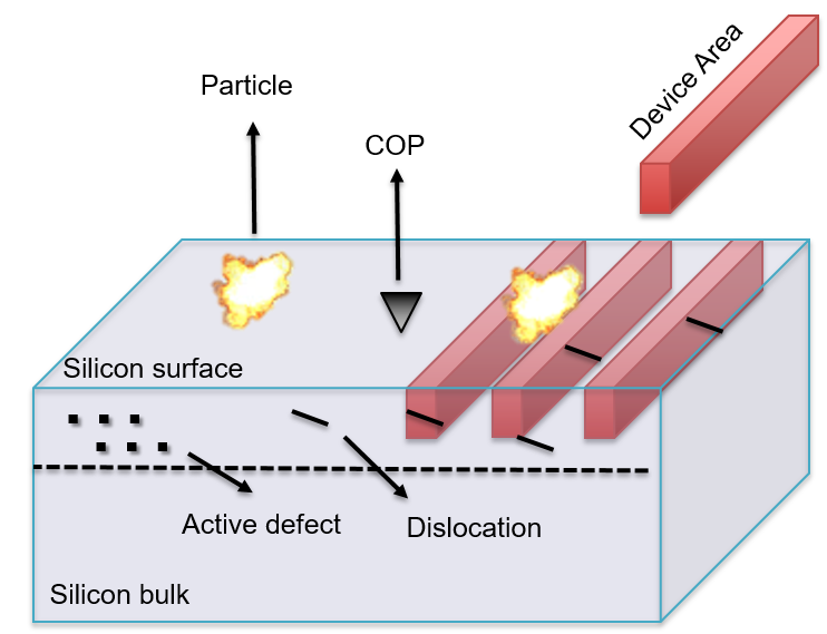 Figure 2. Measurement theory
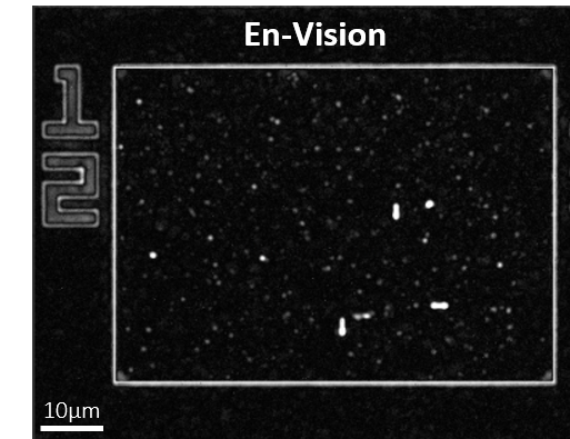
Figure 3. Band to band PL image
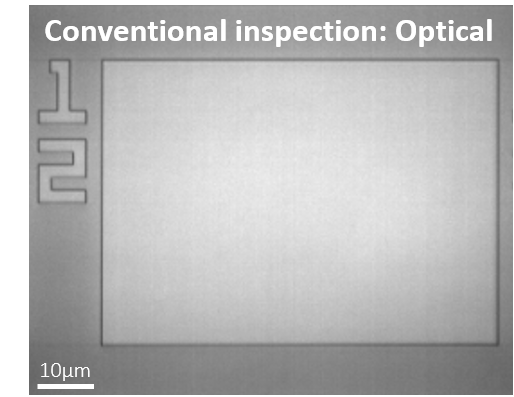
Figure 4. Reflection image
En-Vision detects radiative emission (photoluminescence) of the buried defects. Thus enables detection of defect sizes that are far smaller than the actual optical resolution of the optics in use.
FEATURES
- Non-destructive
- En-Vision sees beyond conventional inspection tools
- Area of interest: active device area (near-surface)
- Enables detection and monitoring of nm scale buried extended defects
- Detection in plain silicon and active device depth
- No expertise needed
Product Line
En-Vision
En-Vision is a new generation inspection system specifically targeting quick and non-destructive detection of nm scale buried defects. Buried defects are located under the silicon surface, invisible to conventional inspection tools (Optical / SEM), and when occurring in the active areas impact device performance and yield.
Products

En-Vision-3000
En-Vision is an essential system for early detection of process-induced dislocations in FEOL, speed-up learning curve for new product / development additionally in-line alternative to chemical etching and X-TEM.
Features and System Specifications:
- Inspected area:
- Product wafers
- Measurement boxes
- In device
- Blanket and monitoring wafers
- Product wafers
- Defects being detected: Buried extended defects (Dislocations, Oi precipitates, COP, Stacking faults and so on)
- Detection limit based on BMD detection of Oi precipitate defects
- Data Acquisition:
- Image segmentation (measurement box and device area)
- Die to die inspection
- Image stitching (larger FOV)
- Data Analysis:
- Statistical tools
- Defect classification
- Batch / Lot Reprocessing
- Data Output: SECS GEM, KLARF, Export
Request Info