


Application
DEFECT INSPECTION
“Bulk Micro Defects” (BMD) is a term commonly used to refer to oxygen precipitates in silicon. In fact, many imperfections in the silicon lattice create defects, and BMDs could be any imperfections including oxygen precipitates, voids, inclusions and so on.
BMDs go by many names, referring to the problems they cause, how they were created, or their physical characteristics. Examples include COPs (Crystal Originated Particles) and Grown-In Defects.
Dislocations can be formed during crystal growth, but also at thermal processing of wafers, during CMOS device manufacturing, like epitaxial layer growth and implant anneal steps.
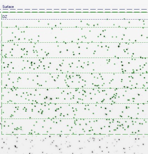 Figure 1. Bulk Micro Defects
Imperfections in the lattice of a semiconductor and impurities create energy states in the bandgap, decrease carrier lifetime, and increase junction leakage. They also act as gettering sites, at which impurities tend to concentrate. The profile of the BMDs is often controlled as shown in Figure 1. by a complex series of high temperature processes to create a “denuded zone”. By this, the surface layer silicon, where the MOS transistor action takes place is free of oxygen precipitates, and the oxygen precipitates in the underlying silicon act as a gettering site to keep impurities away from the MOS transistors.
IR light penetrates most semiconductor materials, and since BMDs alter the local optical properties of a semiconductor, BMDs can be detected by illuminating a sample with IR light and looking at it with a camera that is sensitive to IR.
Technology
POLARIZED INFRARED IMAGING
The Polarized Stress Imaging (PSI) technology is suitable for classifying Si wafers or Si slugs before wafer based on measurement of IR light depolarization.
Examples of varios defect types that can be found in the crystalline material:
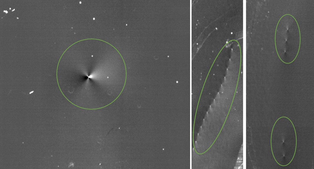
Figure 2. Dislocations
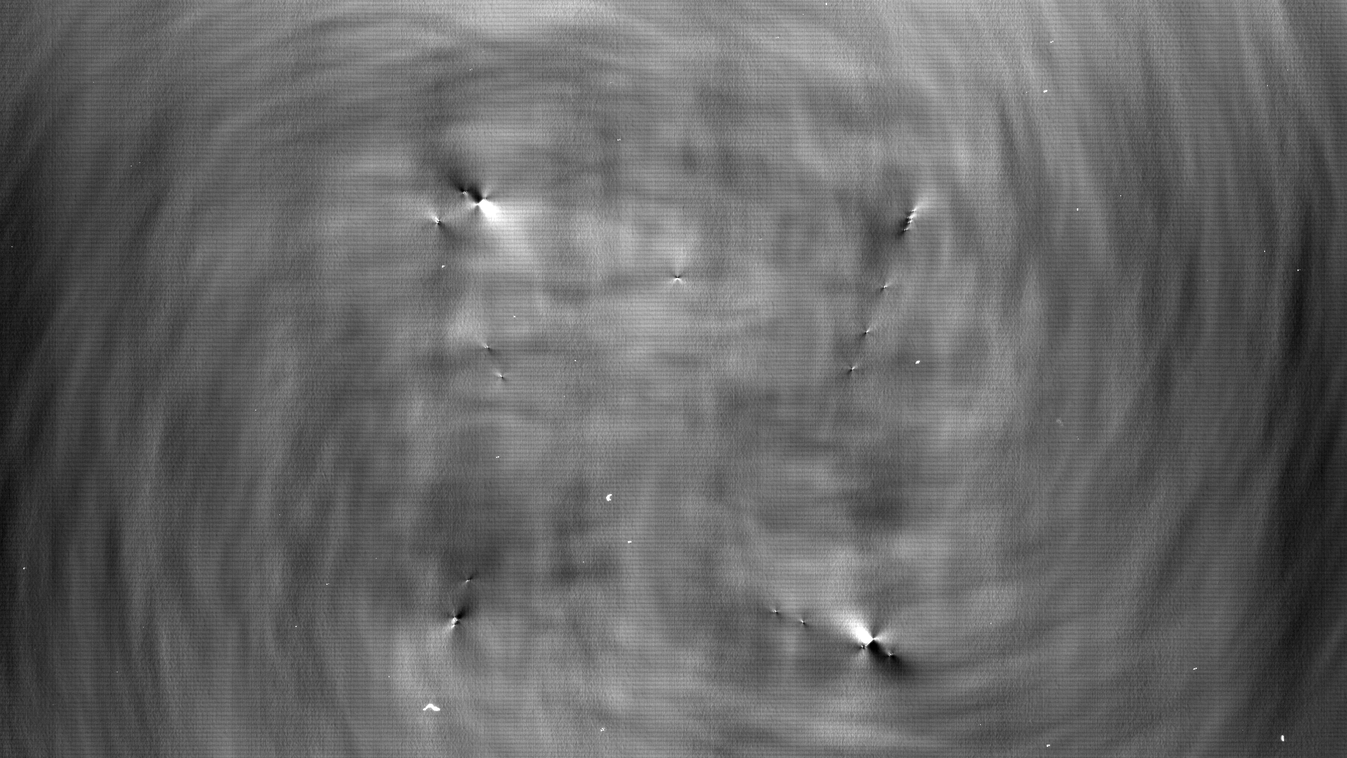
Figure 3. Dislocations
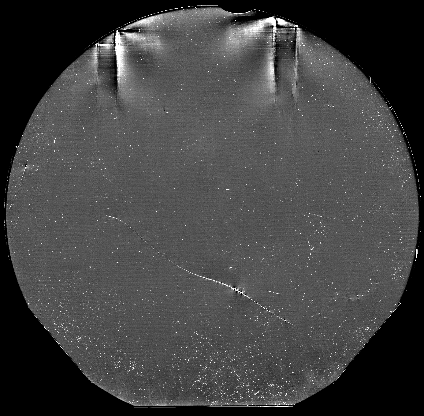
Figure 4. Slip line - Sress image

Figure 5. Slip line - Automatic defect mask
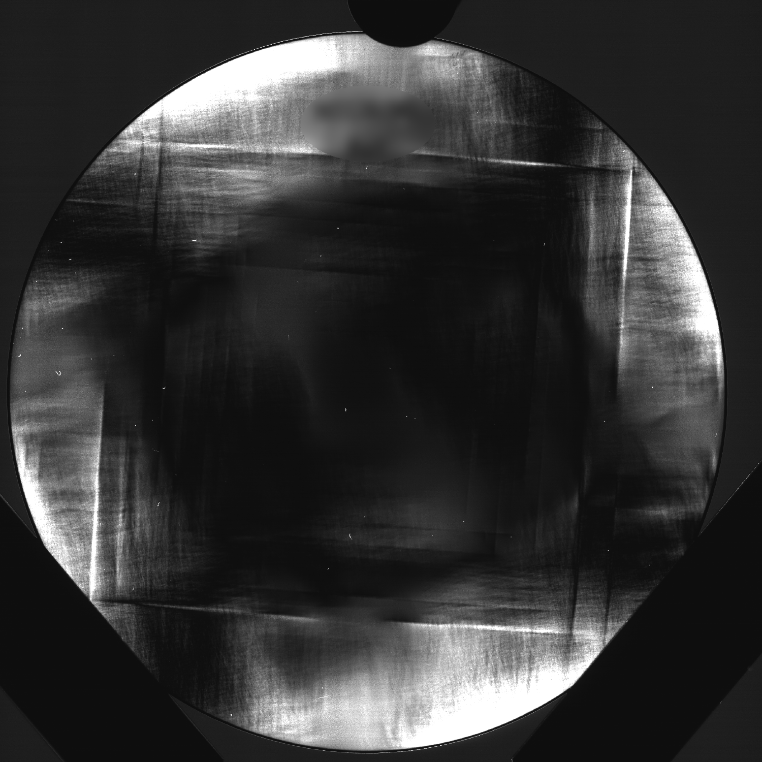
Figure 6. Slip lines
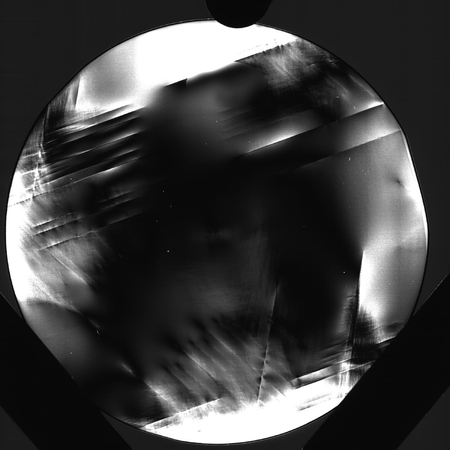
Figure 7. Slip lines
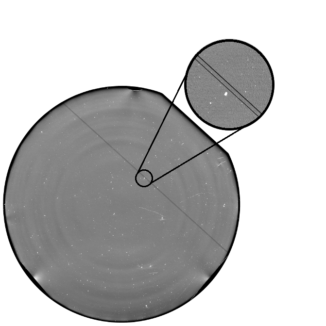
Figure 8. Twin lines
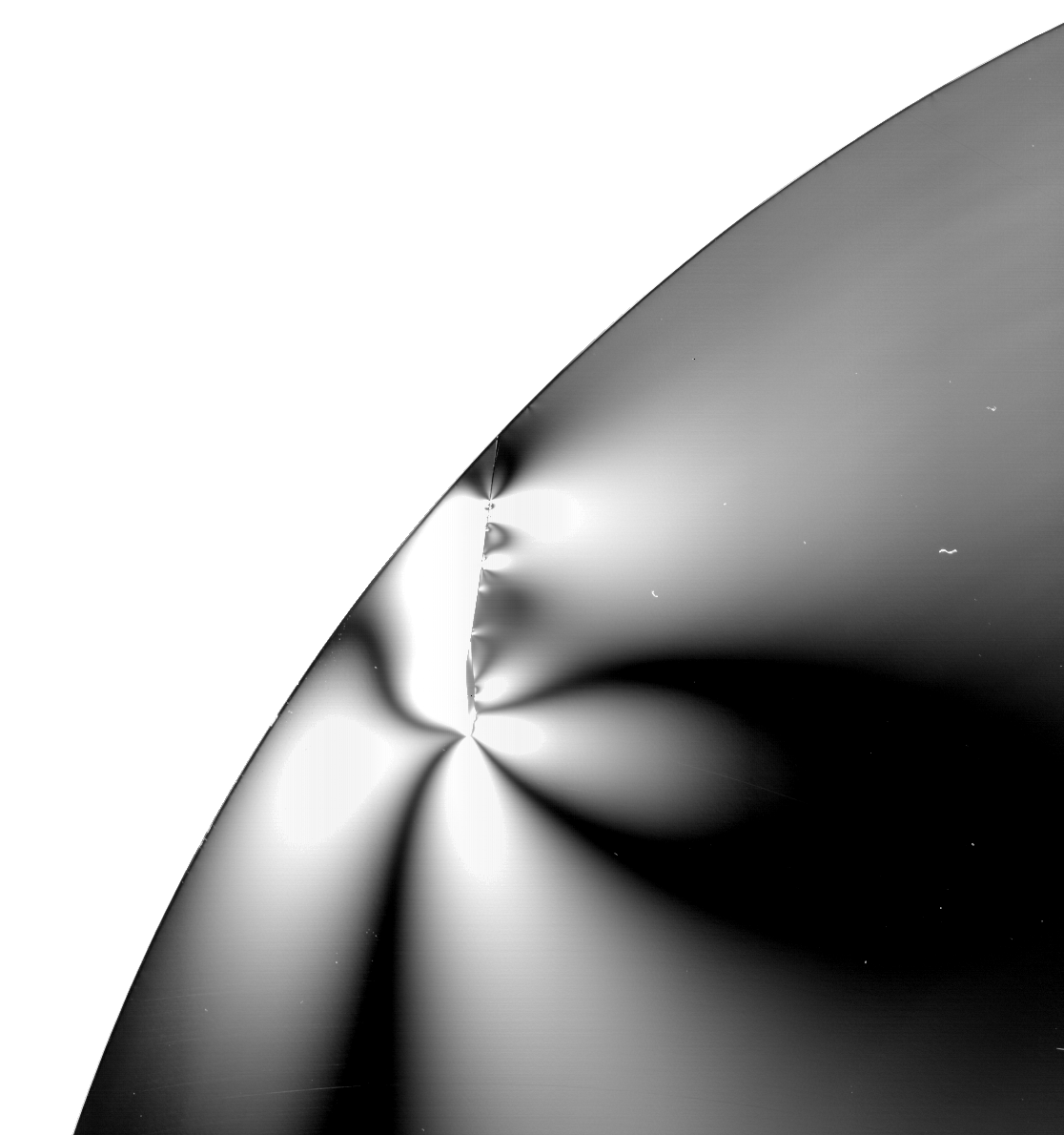
Figure 9. Cracks
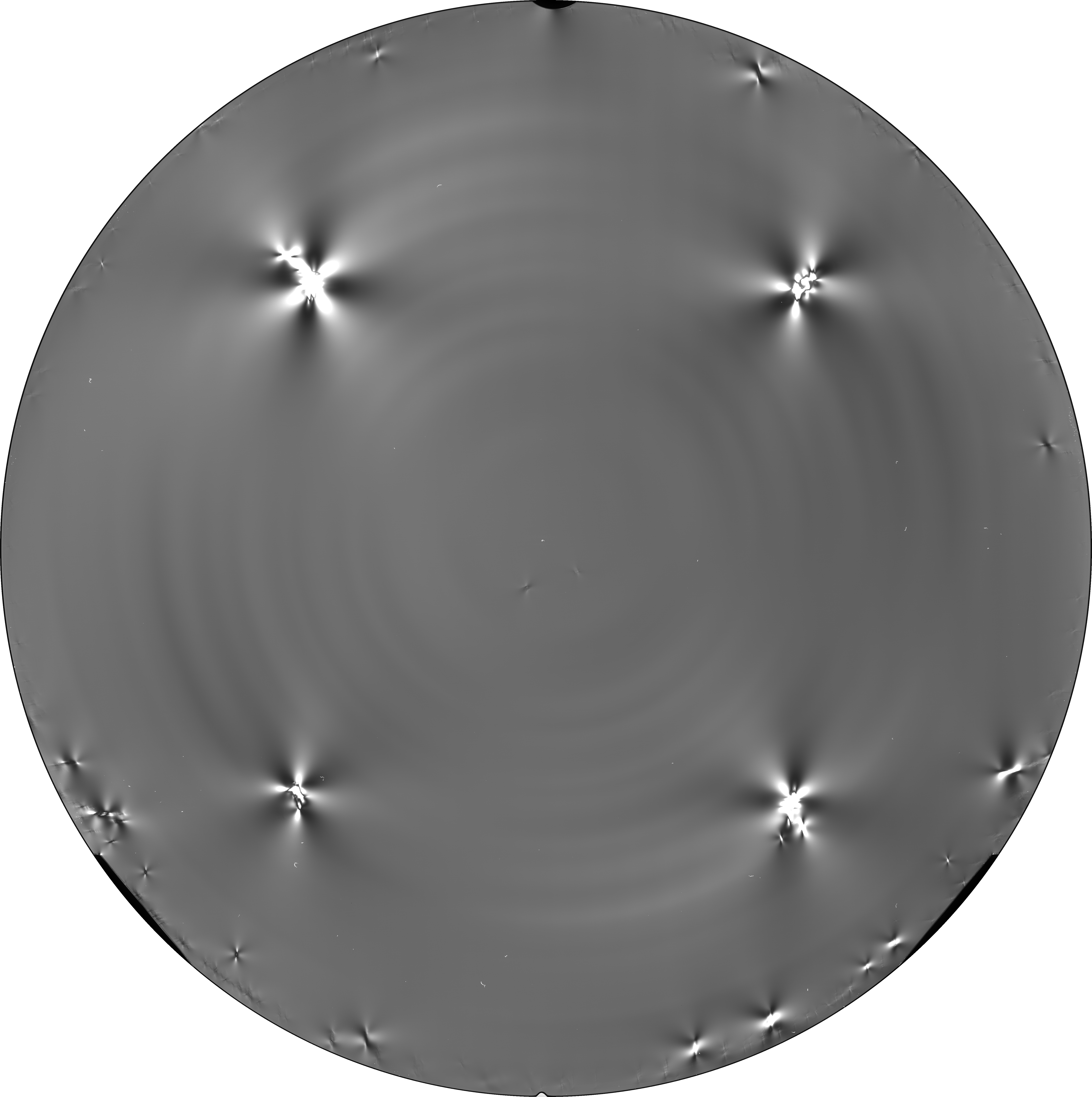
Figure 10. Epi process caused edge defects
The principle of the measurement is the detection of the depolarization with an imaging system.
The light coming from an IR source is projected onto the Si sample through a polarizer. Then the light passes through the Si wafer. At the lower side of the wafer, there is an additional polarizer (analyzer) placed, which is aligned perpendicularly to the initial polarizer. The resulting depolarization signal caused by the stress fields in the wafer is detected by the camera.
Surface particles also depolarize light, due to enhanced light scattering. The detection of these particles on both sides of the sample is realized by the separate optical setup/unit, which is available in the tool.
EVALUATION OF THE MEASUREMENT:
Image is acquired at parallel polarizers. Light intensity: Pp (parallel)
Image is acquired at crossed polarizers. Light intensity: Pc (crossed)
Depolarization can be calculated:
D = 1-(Pp-Pc)/Pp+Pc
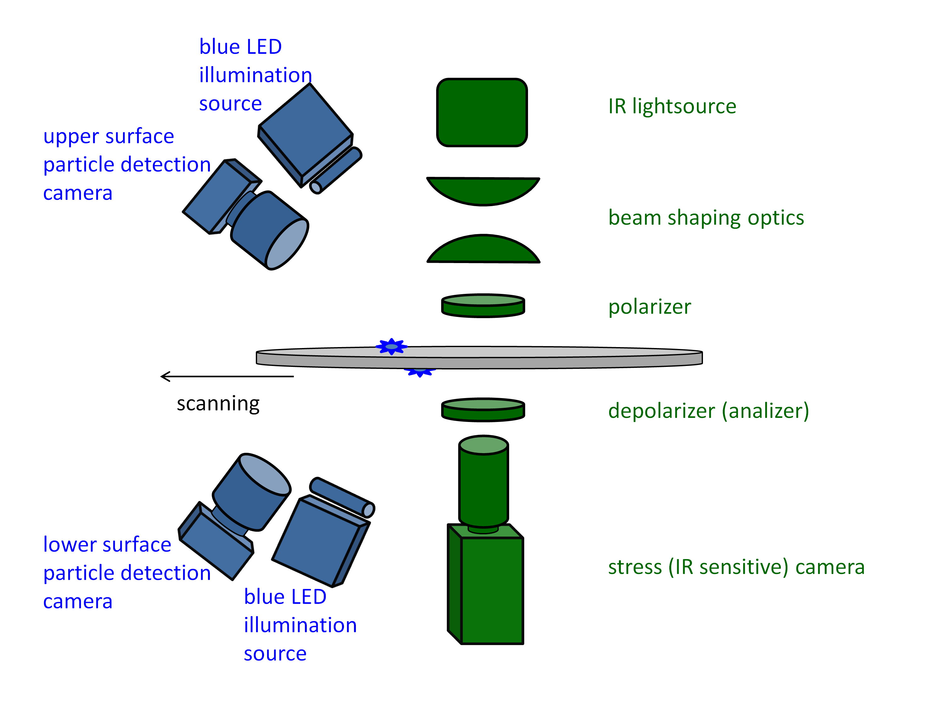 Figure 11. Optical path
Depolarization is a dimensionless quantity. Since D is a small value (Pp >> Pc), it is usually expressed in DU (Depolarization Units): 1 DU = 10-6. Depolarization is related to the retardation of the transmitted wave, therefore it is proportional to the stress expressed by the stress-optic law. In case of bare Si wafers, the transmission is usually homogeneous over the wafer at the parallel polarizers, the calculation of depolarization is not necessary. For the automatic detection of the defects the crossed polarizer image acquisition is sufficient.
OUTPUT OF THE MEASUREMENT:
- Original stress image (or DU map, if calculated)
- Defect map (black and white image highlighting the defects)
- Calculated defect area (full wafer and segmented defects)
- Coordinates of segmented defects (central point of localized and extended ones)
- DU (max, mean) statistics if DU map was calculated.
FEATURES
- Non-contact
- Non-destructive
- Defect detection inside the wafers by transmission method
- Full wafer mapping with high resolution
Product Line
PSI
Defects generated during epitaxy process are also detected by PSI systems with egde grip handling.
- Manual or automatized wafer loading
- Easy wafer edge finding
- Adjustable filtering of the large scale structures
- Automatic defect finding and reporting
- Optional particle detection measurement on both sides parallel to the stress measurement
Products

PSI-3000 Polarized Stress Imaging System
The PSI product line is developed for the automated fabs with high capacity and is specialized for the inspection and visualization of crystal defects related to mechanical stress in Si wafers or slugs.
Features and System Specifications:
- SAM2™ (Semilab Automation Manager 2) user interface compliant to SEMI® standard (E95-0200)
- High precision robot for 300 mm wafers with selectable edge-grip or backside contact end effector
- Option: dual side particle detection on surface
| PSI-3000 | |
|---|---|
| Wafer size | 150 mm / 200 mm / 300 mm |
| Loading | Automatic for one selected sample size Manual loading for one or two additional diameters |
| Platform | Dual FOUP load port capability, SECS/GEM and OHT |
Applications:
- Detection of crystal defect related stress fields in as-grown Si wafers or slugs before wafer state.
- Defect types:
- Localized dislocations
- Slip lines
- Twin lines
- Epi process caused edge defects
Request Info