


Application
OFFLINE PROCESS CONTROL
The best quality control can be achieved by inline process monitoring to check every wafer in the manufacturing process. However, in some cases the short cycle time (usually less than 1 second) does not allow to realize detailed analysis of the wafer, which may include full wafer mapping and techniques requires mechanical contacts.
The measurement tools were designed to include non-destructive techniques and favor non-contact methods where possible.
- Fast measurements
- User friendly operation
- Low cost of ownership
The applications include the followings:
- Incoming wafer characterization
- Measurement of electrical parameters in different manufacturing steps
- Characterization of deposited layer parameters
- Monitoring surface passivation efficiency and homogeneity
Technology
SHEET RESISTANCE MEASUREMENT
The combination of the ion implant process and the process to anneal implants is usually monitored by measuring the sheet resistance of the implanted layer. The sheet resistance varies with dose, energy, and the amount of implanted species that has become electrically active. It is the sheet resistance that ultimately determines the device performance. Thus, measuring sheet resistance is an excellent way to monitor everything associated with an implant process.
The basic idea of the JPV method is the light excitation of the np or pn layer structure, and the pick-up of the resulting junction photovoltage by a capacitive probe. The detected potential is determined by the sheet resistance of the implanted layer, capacitance of junction and resistance through over the diode.
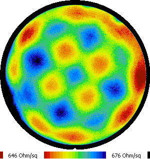
Figure 2. Sheet resistance measurement (lower range)
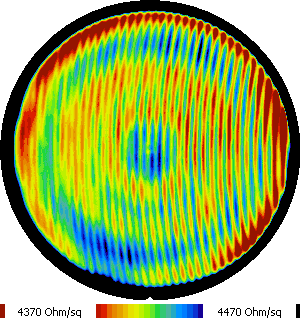
Figure 3. Sheet resistance measurement (higher range)
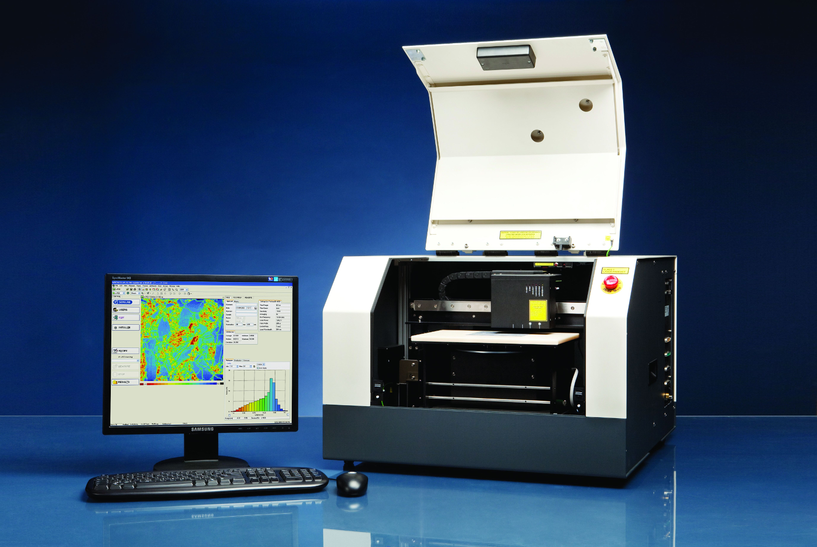
Semilab offers JPV technology to make non-contact, high resolution fast maps of sheet resistance.
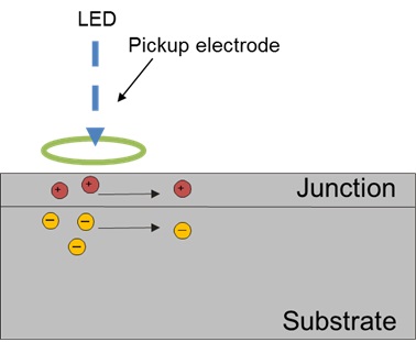
Figure 4. Measurement theory
MEASUREMENT THEORY:
The sample is illuminated by chopped LED light, which generates electrons and holes in the substrate layer. The generated charge carriers diffuse to the junction and the electric field located in the junction separates them. The result of the separation is the change in the junction voltage. This voltage change spread laterally in the implanted layer and the attenuation depends on the sheet resistance, junction capacitance, resistance of the junction and chopping frequency of the LED.
The potential change is detected by a capacitive sensor in order to evaluate the JPV signal, as a function of the frequency of the emitted light.
Based on the evaluation, the sheet resistance (Rs), capacitance of junction (Cd) and the resistance of the diode (Rd) can be calculated.
The junction leakage current is directly connected to the Rd by the following equation:
I_L=kt/q/R_d
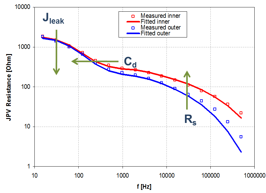
Figure 5. The detected potential is determined by Rs, Cd, Rd and frequency
FEATURES
- Non-contact, non-destructive
- No probe conditioning
- No sample preparation needed
- Works through oxide or coating
- High resolution mapping capability
- Fast mapping
- Good repeatability
Product Line
SHR, WT, PV
Metrology systems for quality assessment and determination of defects in silicon PV wafers.
Products

SHR-1000
SHR-1000 is a fast, non-contact and reliable alternative of four point probe in the characterization of emitter layers. Emitter sheet resistance is a primary quality control parameter for silicon cells in PV applications.
Features and System specifications:
- Non-contact
- Preparation free
- Applicable on coated samples (phosphorous glass)
- High speed
- Production line compatible
- Alternative method to the traditional four-point-probe
- Detection of shunts
- Including software and PC
- High speed
- Production line compatible
- Optional reflectance measurement
- Range: 10-200 Ω/sq

PV-2000A
Features and System specifications:
It is a new integrated platform with the following capabilities:
- SPV Diffusion Length
- Discrete ites and mapping of incoming and processed wafers to final cells.
- UV/Blue SPV ratio for surface passivation (arb. units)
- Monitorable parameters:
- Diffusion length (L)
- Fe contamination (Fe)
- Other Recomb. Centers (NR)
- LID Defect Contamination
- Noncontact C-V profiling
- Time resolved approach with leakage correction
- Monitorable parameters:
- Flatband Voltage (Vfb)
- Oxide Total Charge (Qtot)
- Interface Trapped Charge (Qit)
- Interface Trap Density (Dit)
- Dielectric Capacitance (CD) and thickness (CET),
- Dielectric Leakage and PID testing 3 to 1000 nm planar and textured films
- Accelerated LID testing
- Temperature stages (20-220°C), 2 illumination stations (halogen and flash); robotic handling: activates/deactivates iron and/or boron-oxygen
- LID defects in minutes
- ALID is sequenced with SPV for Fe and LID defect mapping in short time
- Applicable to wafers and solar cells
- QSS-μPCD
- Discrete sites and mapping of incoming and processed wafers
- PCD laser wavelength: 904 nm
- Monitorable parameters:
- Decay lifetime (τ eff.d)
- Steady-state lifetime (τ eff.ss)
- Injection level (Δn)
- Effective surface recombination (Seff)
- QSS light intensity: 0.005 to 30 Suns
- Emitter Saturation Current (J0)
- Implied Voc
- Light Beam Induced Current (LBIC)
- Mapping of solar cells 1 to 4 lasers
- Measurement parameters: Current; Diffusion Length; Reflectance; Internal Quantum Efficiency (IQE)
- Reflectance measurement and IQE mapping
Other testing capabilities:
- SPV Surface Lifetime
- SPV Mapping of Rshunt and Voc
- Noncontact Suns-Voc
- Wafer Thickness Measurement

WT-2000PVN
The WT-2000PVN is a table top measurement system, capable of performing a variety of measurements on PV cells, wafers, and blocks. The base system includes the overhead functions, and you configure the measurement capabilities to match your specific needs, by selecting from the options below.
The WT-2000PVN can measure blocks and ingots, as well as wafers and cells. For measuring wafers and cells, people typically produce maps. When measuring blocks or ingots, people often produce only line scans, to save time, WT-2000PVN can do both.
Most producers of PV cells own a WT-2000PVN. It is extremely useful for:
- Engineering development and characterization
- Batch testing of production
- Comprehensive troubleshooting of production problems
Measurement techniques that can be integrated in WT-2000PVN:
- µ-PCD / carrier lifetime
- Measured parameter: carrier lifetime
- High resolution mapping and discrete point measurements
- SHR / sheet resistance
- Measured parameter: emitter sheet resistance
- Mapping and discrete point measurements
- LBIC / photovoltaic response, quantum efficiency, diffusion length
- High resolution mapping with 1 to 4 lasers
- Measured parameters:
Short circuit current
Direct and scattered reflectance
IQE and EQE
Diffusion length
- Eddy current
- Non-contact resistivity mapping
- Different resistivity range probes
- Bias light to µ-PCD