


Application
Technology
NON-CONTACT C-V PROFILING
Semilab SDI FAaST systems represent state-of-the-art non-contact electrical metrology used in manufacturing control and development of semiconductor devices and materials. Employing non-contact surface potential probing techniques combined with illumination and/or non-invasive surface charging, these powerful techniques measure a broad range of parameters characterizing semiconductor wafers, dielectrics and interfaces with astounding precision, while saving the cost and time involved in fabricating dedicated test devices.
The major application of the Non-Contact C-V profiling metrology is monitoring of dielectrics during IC manufacturing. The most important feature, differentiating it from conventional electrical measurements, is its preparation free non-contact nature, which eliminates preparation of MOS capacitors, thereby reducing metrology cost and facilitating fast data feedback in both Manufacturing and R&D environments.
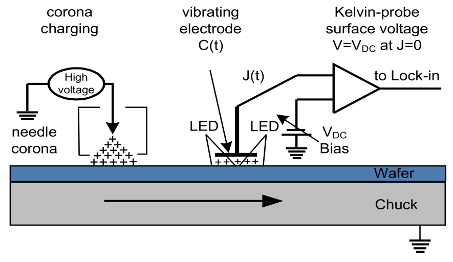
The non-contact corona-Kelvin metrology uses corona discharge in air to place an electric charge on a semiconductor wafer. The wafer response is monitored with a vibrating capacitor probe, typically a Kelvin-probe, which measures the surface voltage (Vcpd). Surface voltage monitoring in both the dark and under strong illumination enables separation of two important voltage components:
- Dielectric voltage (VD)
- Semiconductor surface potential (Vsb)
Analysis of the acquired charge-voltage data provides electrical parameters such as Dit, Vfb, Qtot (dielectric charge), CD, EOT, and Dielectric Leakage.
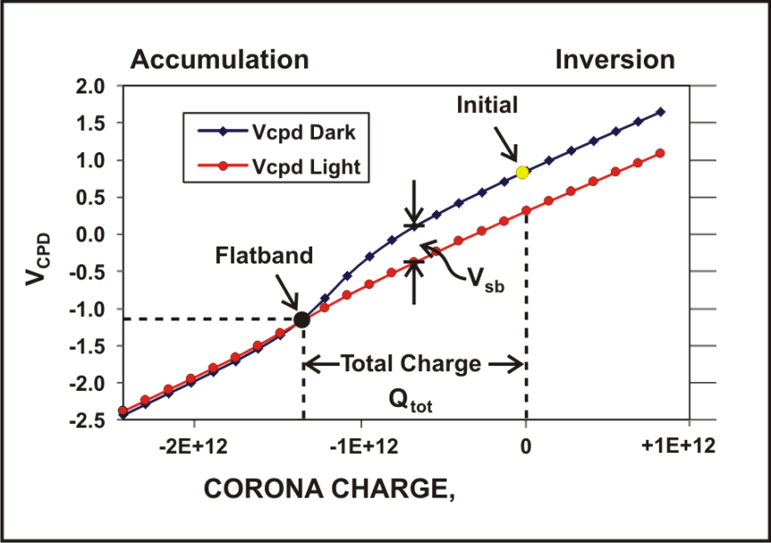
Example Vcpd vs Qcorona data for dielectric on p-type Si
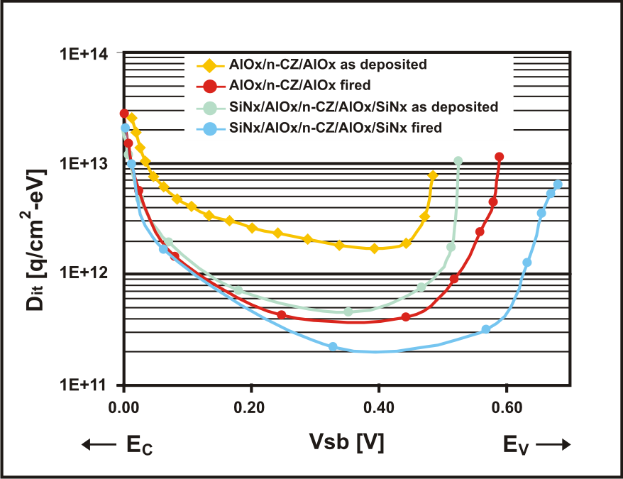
Example Dit spectra for various dielectrics on Si
The major application of this metrology is monitoring of dielectrics during IC manufacturing. The most important feature, differentiating it from conventional electrical measurements, is its preparation free non-contact nature, which eliminates preparation of MOS capacitors, thereby reducing metrology cost and facilitating fast data feedback in both Manufacturing and R&D environments.
FEATURES
- Non-contact electrical C-V and I-V metrology providing characterization of dielectrics and interfaces with unparalleled accuracy and precision for the IC manufacturing and R&D environment
- Available in Macro configuration for measurements on Monitor wafers
- Unique Micro configuration option using Kelvin Force Microscopy (KPFM) measures C-V and I-V characteristics in scribe-line test sites and in active device areas on Production wafers
- Demonstrated inter-fab Tool to Tool Matching
- Time-resolved voltage measurements enable dielectric leakage determination and corresponding leakage-corrected true C-V curve measurement for sub-nanometer dielectrics
- Proprietary C-V simulator for dielectric capacitance extraction that works in the presence of very large interface trap density
- Proven applications for advanced ultra-thin dielectrics, high k dielectrics, and inter-layer dielectrics
- Excellent correlation to End-Of-Line device data
Product Line
FAaST
FAaST metrology includes best in the world Semilab SDI unique capabilities:
- The Digital Surface PhotoVoltage, DSPV, measurement of minority carrier diffusion length with unmatched sensitivity for Fe detection in Si wafers.
- Corona-Kelvin characterization of dielectrics and interfaces with capability for pattern wafer measurement and micro-scale scribe-line (SL) measurement using micro-corona and Kelvin Force Probe Microscopy (KPFM).
- Wafer mapping is available for all measured parameters and especially high-throughput mapping of non-visual defects including electrical charge defects caused by plasma etching, ion implantation, or mobile ion contamination.
Semilab SDI FAaST system’s offer:
- Flexible configurations that can be customized to suit individual customers’ needs.
- Platforms range from a fully automated dual 300mm loadport system configured with all measurement options and capable to meet the 300mm Semi requirements of modern IC Fabs to manual load systems configured with a single measurement technology that can measure samples as small as ~20mm x 20mm making them well suited for the University or Laboratory environment.
Products

FAaST 300-SL
The FAaST 300 SL system is the cutting-edge non-contact electrical metrology system that combines both of Semilab SDI’s patented Micro and Macro corona-Kelvin methods into a single platform designed to support advanced R&D as well as the most demanding high-volume manufacturing environment.
Features and System specifications:
- Automatic robotic wafer handling
- Dual FOUP Loadport; optional configuration with single Loadport or including Versaport
- Suitable for patterned wafer (Micro) and monitor wafer (Macro) measurements
- Semilab SDI patented high resolution (10µm) Micro corona-Kelvin based on Kelvin Probe Force Microscopy (KPFM) for measurement of dielectric and interface properties in Scribe Line test sites (down to 40µm x 40µm) and active device regions
- Advanced 2 step Non-Visual Defect (NVD) Inspection that combines full wafer Macro surface voltage imaging and focused high resolution intra-die surface voltage imaging using KPFM
- Automatic programmable sites or contour mapping of dielectric properties including:
- Dielectric Capacitance (CD) and Thickness (EOT),
- Dielectric Leakage Current (I-V)
- Flatband Voltage (Vfb),
- Interface Trap Density (Dit),
- Interface Trapped Charge (Qit),
- Semiconductor Surface Barrier (Vsb),
- Oxide Total Charge (Qtot),
- Mobile Ionic Charge (Qm), among others
- FAaST software package; including Measurement, Recipe Writing and Data Viewing applications
- Suitable for measurement on: semiconductors (e.g. Si, SiGe, InGaAs, SiC, GaN) with high-k and low-k dielectric films (e.g. SiO2, SiNx, Al2O3, HfO2 ; mixed dielectrics and dielectric film stacks)
- Default configuration for 300mm wafers; with option for 200mm/300mm bridge configuration
- Line Conditioner with flexible compatibility
- Compatible for configuration with other Semilab SDI FAaST tool measurement technologies
- Additional available options include: Mini-environment, 300mm Semi compliant Automation, Seismic brackets, wafer OCR, RFID, cassette barcode reader, 1000V Vcpd measurement range

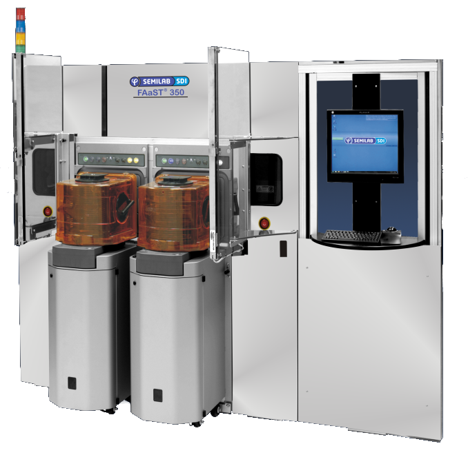
FAaST 350 C-V / I-V
The FAaST 350 C-V / I-V system applies Semilab SDI’s advanced C-V / I-V measurements based on patented corona-Kelvin methods to non-contact imaging of dielectrics and interface properties. This workhorse platform is designed with automated wafer handling from dual FOUP Loadport loading stations fully capable of supporting in-line measurements in the most demanding high-volume manufacturing environment.
Features and System specifications:
- Automatic robotic wafer handling
- Dual FOUP Loadport; optional configuration with single Loadport or including Versaport
- Full wafer Non-Visual Defect (NVD) Inspection and Plasma Damage Monitoring using Surface Voltage FAST Mapping mode
- Automatic programmable sites or contour mapping of dielectric properties including:
- Dielectric Capacitance (CD) and Thickness (EOT)
- Dielectric Leakage Current (I-V)
- Flatband Voltage (Vfb)
- Interface Trap Density (Dit)
- Interface Trapped Charge (Qit)
- Semiconductor Surface Barrier (Vsb)
- Oxide Total Charge (Qtot)
- Mobile Ionic Charge (Qm), among others
- FAaST software package; including Measurement, Recipe Writing and Data Viewing applications
- Suitable for measurement on: semiconductors (e.g. Si, SiGe, InGaAs, SiC, GaN) with high-k and low-k dielectric films (e.g. SiO2, SiNx, Al2O3, HfO2 ; mixed dielectrics and dielectric film stacks)
- Default configuration for 300mm wafers; with option for 200mm/300mm bridge configuration
- Line Conditioner with flexible compatibility
- Compatible for configuration with other Semilab SDI FAaST tool measurement technologies
- Additional available options include: Mini-environment, 300mm Semi compliant Automation, Seismic brackets, wafer OCR, RFID, cassette barcode reader, 1000V Vcpd measurement range

FAaST 330/230 C-V / I-V
FAaST 330/230 C-V / I-V systems apply Semilab SDI’s advanced C-V / I-V measurements based on patented corona-Kelvin methods to provide non-contact imaging of dielectric and interface properties on monitor wafers. These platforms include automated wafer handling that is suitable for the medium to high-volume manufacturing environment. These models feature:
- Automatic robotic wafer handling
- Single open-cassette wafer loading station; with configurable options including SMIF / FOUP Loadport / Versaport
- Full wafer NVD inspection and Plasma Damage Monitoring using Surface Voltage FAST Mapping mode
- Automatic programmable sites or contour mapping of dielectric properties including:
- Dielectric Capacitance (CD) and Thickness (EOT)
- Dielectric Leakage Current (I-V)
- Flatband Voltage (Vfb)
- Interface Trap Density (Dit)
- Interface Trapped Charge (Qit)
- Semiconductor Surface Barrier (Vsb)
- Oxide Total Charge (Qtot)
- Mobile Ionic Charge (Qm), among others
- FAaST software package; including Measurement, Recipe Writing and Data Viewing applications
- Suitable for measurement on: semiconductors (e.g. Si, SiGe, InGaAs, SiC, GaN) with high-k and low-k dielectric films (e.g. SiO2, SiNx, Al2O3, HfO2 ; mixed dielectrics and dielectric film stacks)
- Configurable for 100mmto 300mm wafers, with options available to accommodate multiple wafer sizes and to allow for manual load of smaller wafer diameters
- Line Conditioner with flexible compatibility
- Compatible for configuration with other Semilab SDI FAaST tool measurement technologies
- Additional available options include: Mini-environment, 300mm Semi compliant Automation, Seismic brackets, wafer OCR, RFID, cassette barcode reader, 1000V Vcpd measurement range

FAaST 310/210 C-V / I-V
FAaST 310/210 C-V / I-V systems apply Semilab SDI’s advanced C-V / I-V measurements based on patented corona-Kelvin methods to provide non-contact imaging of dielectric and interface properties on monitor wafers. The platforms are suitable for R&D and low-volume manufacturing environments. These models feature:
- Manual wafer loading; including cassette placement station and vacuum wand
- Full wafer NVD inspection and Plasma Damage Monitoring using Surface Voltage FAST Mapping mode
- Automatic programmable sites or contour mapping of dielectric properties including:
- Dielectric Capacitance (CD) and Thickness (EOT)
- Dielectric Leakage Current (I-V)
- Flatband Voltage (Vfb)
- Interface Trap Density (Dit)
- Interface Trapped Charge (Qit)
- Semiconductor Surface Barrier (Vsb)
- Oxide Total Charge (Qtot), among others
- FAaST software package; including Measurement, Recipe Writing and Data Viewing applications
- Suitable for measurement on: semiconductors (e.g. Si, SiGe, InGaAs, SiC, GaN) with high-k and low-k dielectric films (e.g. SiO2, SiNx, Al2O3, HfO2 ; mixed dielectrics and dielectric film stacks)
- Configurable for 50mm to 300mm wafers, with options available to accommodate multiple wafer sizes
- Step Down Power transformer with flexible compatibility
- Additional available options include: Automatic data upload and/or data export, Seismic brackets