


Application
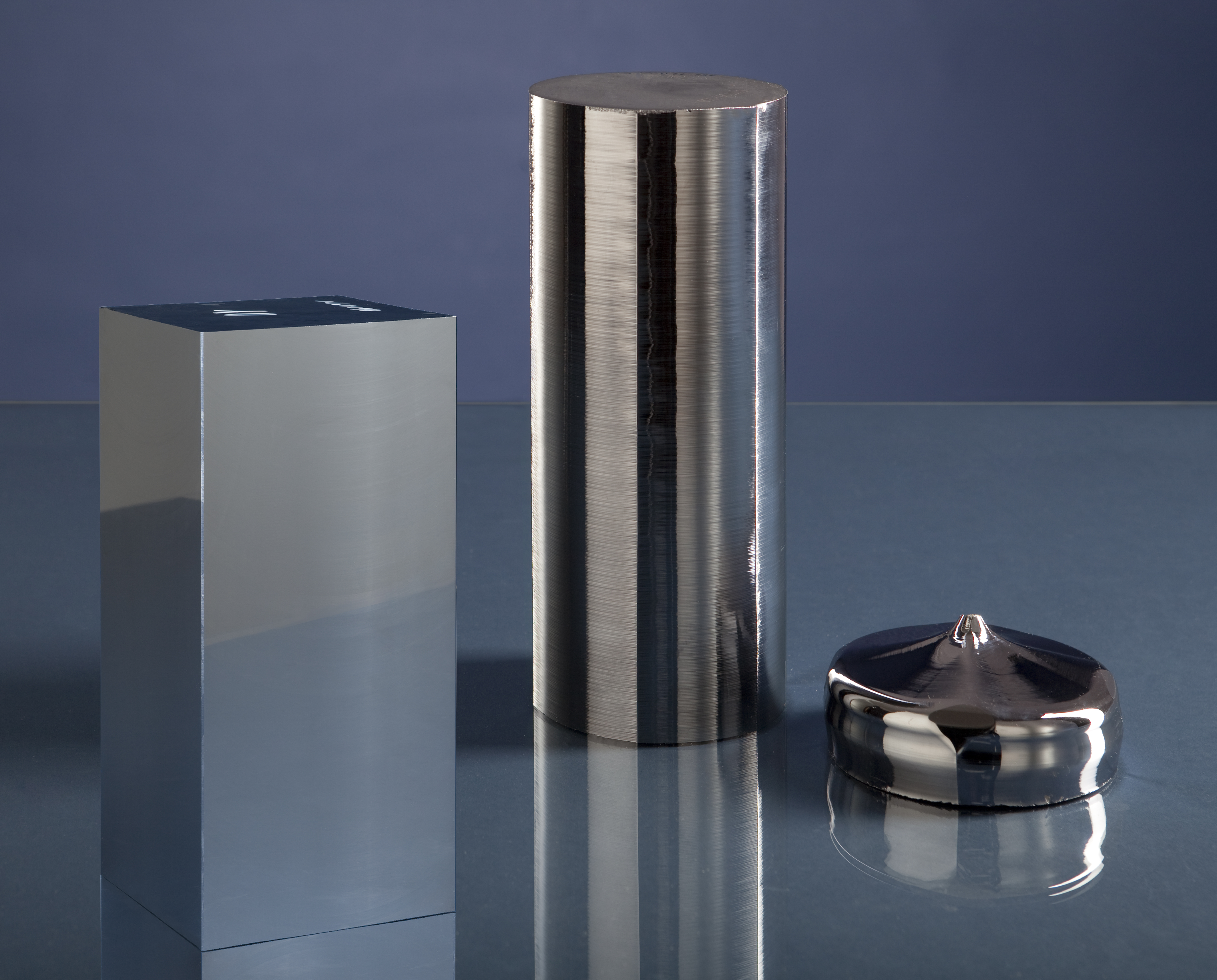
SI INGOT/ BLOCK TESTING
The quality of the silicon crystal determines the maximum achievable conversion efficiency of the final photovoltaic device. Thus, the quality control of the as-grown Si crystals is crucial to stabilize the manufacturing of modern Si solar cells. Semilab offers various solutions to control all the important material parameters in both multi- and monocrystalline silicon ingots.
Resistivity of the mono and multicrystalline ingots is tested by using eddy current sensor, integrated into various system platforms.
Metallic contamination and extended crystal defects are detected by using different versions of PhotoConductance Decay and Photoluminescence methods.
Finally, our Infrared Imaging system localizes the larger precipitations in the crystal in order to prevent the failures in the wire sawing process.
Technology
BULK RESISTIVITY MEASUREMENT
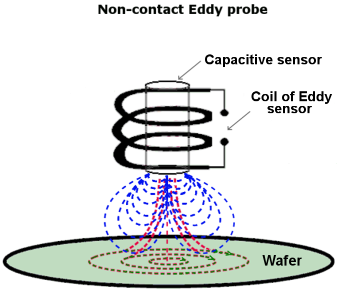
Bulk Resistivity Measurement of silicon wafers, ingots and blocks can be realized with help of non-contact, non-destructive Eddy current technique. When AC current flows in a coil, it' s magnetic field induces circulating (Eddy) currents in the sample. The Eddy current measurement is actually the measurement of the electrical loss in the material. The measuring head moves above the sample in constant height without touching of it. Because the measured signal depends on sample resistivity, thickness, and distance between the probe and sample, there is built-in distance sensor (based on capacitance measurement), which measures in the same spot like Eddy sensor. From the distance value and the Eddy signal, true resistivity values can be obtained.
The measured signal (Ueddy) always depends on Distance between the coil and sample, additionally:
- In case of Semi-infinite samples as blocks depends on Resistivity of the material
- In case of Samples with finite thickness as wafers depends on Resistivity and thickness
- In case of Thin layers depends on Sheet resistance
The Eddy current is higher in good conducting material compared to less conductive material.
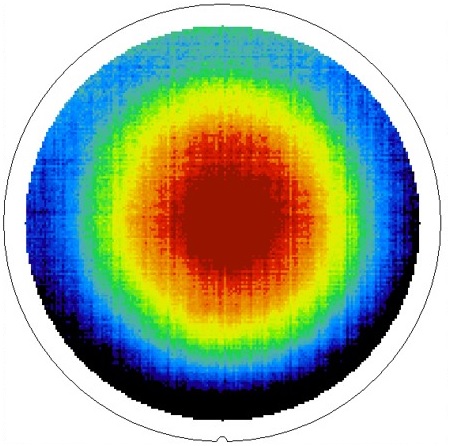
Wafer map
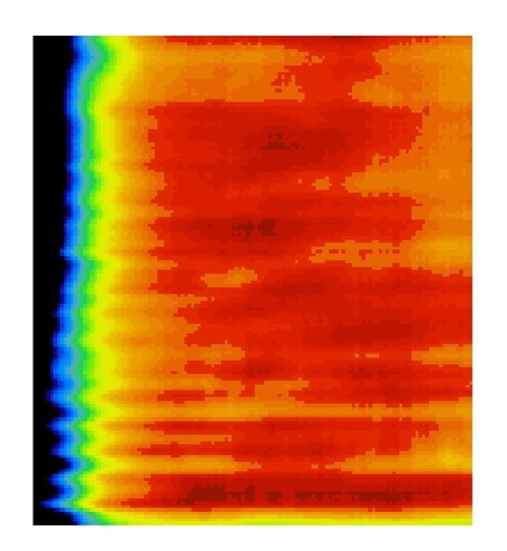
Block map
FEATURES
- Non-contact
- Non-destructive
- Extremely fast
- No sample preparation
Product Line
RT, WT
RT product line consist of products that are capable of measuring different properties of crystalline solar cell material. All of these products are capable of measuring in on point at a time. The position of the measurement is freely chosen by the operator.
The RT family measures resistivity of silicon feedstock material, blocks. Options are P/N tester and wafer thickness measurements.
The WT product line is a powerful measurement platform for performing many different semiconductor material characterization measurements. The base system includes all the overhead functions necessary to perform characterization measurements, including power supplies, computer and operating software, XY measurement stage, etc. The WT-2000 is typically used to make maps, where the wafer is scanned at a programmable raster. Each system is configured to the user’s requirements by adding treatment and measurement capabilities.
Products

RT-110
The Resistivity Tester is a non-contact bulk resistivity measurement tool for rapid classification of silicon wafers. It operates via eddy current technology.
The RT-110 resistivity tester is suitable for measurement of the resistivity and thickness of bare semiconductor wafers. The wafer handling is manual, the measurement starts automatically. The RT-110 can measure in 4 different resistivity ranges. Conductivity type determination is possible by the built-in P/N tester.
Features and System specifications:
- Resistivity range 0.01-20 Ωcm
- Computer controlled operation
- No sample preparation
- Measurement time about 1s (excluding handling)
- Manual wafer loading
Options:
- Wafer Thickness Measurement in the range of 200 to 1000 µm
- Probe for P/N conductivity type testing

RT-1000
The RT-1000 Resistivity Tester based on eddy current technique allows non-contact, non-destructive measurement of bulk resistivity of ingots and blocks as well as rapid classification of feedstock material including single and multicrystalline pieces and pot-scrap.
RT-1000P is a portable version of the resistivity tester that can be used with any computer, using an USB-port.
Features and System specifications:
- Resistivity range 0.01-20 Ωcm (by using two probes with different ranges)
- Computer controlled operation
- No sample preparation
- Measurement time per sample about 1s
- User defined resistivity categories for sorting the samples
- Audible alarm for samples with resistivity out of range
Options:
- Probe head for P/N conductivity type testing

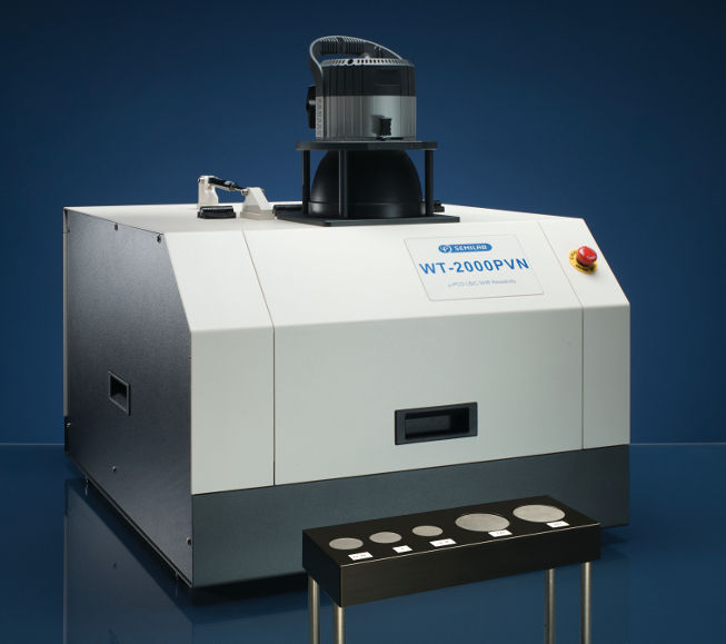
WT-2000PVN
The WT-2000PVN is a table top measurement system, capable of performing a variety of measurements on PV cells, wafers, and blocks. The base system includes the overhead functions, and you configure the measurement capabilities to match your specific needs, by selecting from the options below.
The WT-2000PVN can measure blocks and ingots, as well as wafers and cells. For measuring wafers and cells, people typically produce maps. When measuring blocks or ingots, people often produce only line scans, to save time, WT-2000PVN can do both.
Most producers of PV cells own a WT-2000PVN. It is extremely useful for:
- Engineering development and characterization
- Batch testing of production
- Comprehensive troubleshooting of production problems
Measurement techniques that can be integrated in WT-2000PVN:
- µ-PCD / carrier lifetime
- Measured parameter: carrier lifetime
- High resolution mapping and discrete point measurements
- SHR / sheet resistance
- Measured parameter: emitter sheet resistance
- Mapping and discrete point measurements
- LBIC / photovoltaic response, quantum efficiency, diffusion length
- High resolution mapping with 1 to 4 lasers
- Measured parameters:
Short circuit current
Direct and scattered reflectance
IQE and EQE
Diffusion length
- Eddy current
- Non-contact resistivity mapping
- Different resistivity range probes
- Bias light to µ-PCD