


Application
ELA PROCESS CHARACTERIZATION (LTPS)
Excimer Laser Annealing (ELA) is the key process parameter in Low Temperate Silicon (LTPS) layer manufacturing: ELA determines many important final parameters of the layer and finally of the device: crystallinity, mobility, etc. Semilab developed a combination of metrologies which can easily determines the Optimal Energy Density (OED). This combination is capable to distinguish the properties of two LTPS samples which were annealed with very similar annealing parameters. Using this feature fine tuning of ELA process is easy and fast and does not require any macro inspection with human decision.
Furthermore using our contact 6pp the sheet resistance can be determined as well.
Technology
CHIP QUALITY (LINE MURA AND µ-PCR)
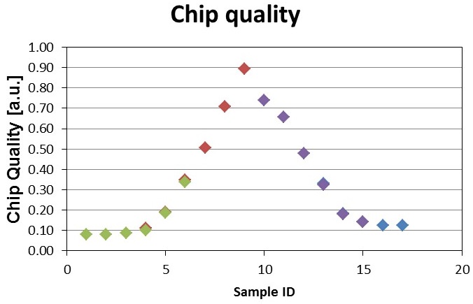
Chip quality measurement method is a combination of the electrical Microwave Photoconductive Response (μ-PCR) and the optical LineMura metrologies, where the result is a function of measured values which describes the quality of the thin film.
The „Chip quality” - chip (or device) is a selected area unit on the production plate - is a weighted, normalized sum of the μ-PCR and LineMura parameters.
Normalization for μ-PCR Amplitude, Lifetime 1-2 and LineMura Brightness:
- Normalized value = Raw value/Normalization factor
Normalization for LineMura relative deviation values:
- Normalized value = Normalization factor/Raw value
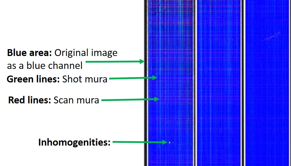
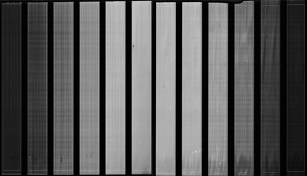
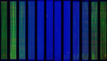
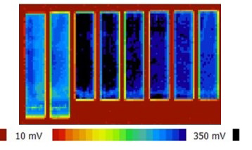
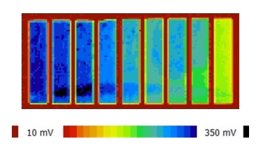
Line Mura is an optical method for characterization of an LTPS layer - low temperature poly-silicon thin film - by identifying the Excimer Laser Annealing (ELA) process caused defects and nonuniformities (mura) and the Optimal Energy Density (OED) of the laser. The metrology consists of a flat angle illumination and flat angle camera system.
JUDGMENTS
The following judgments can be defined for production point of view:
The parameter Judgement (Good, Not Good) can be performed for all chips, for each parameter and for the whole panel as well.
The Chip Judgement is performed for each chip, in case of any parameter failed, than the chip judgement is failed.
The Universal Chip Judgement defined for the whole panel: if more chips failed then a predefined number than this universal Chip judgement is failed.
OPTIMAL ENERGY DENSITY
Using the chip quality and the judgment preferences it is possible to determine optimal laser settings for production: the judgments help to neglect bad chips and Chip quality can be used to make an order.
EXCIMER LASER ANNEALING
It is a key process to fabricate high-quality poly-silicon (p-Si) thin films for use in flat-panel displays. The laser line beam is scanned over a thin (typical 50 nm) amorphous silicon (a-Si) film, which absorbs the UV radiation, got partially melted and is converted from amorphous to polycrystalline silicon at temperatures as low as 200°C. This process provides more than hundred times higher electron mobility than that of a-Si.
One of the most important parameters of the process is the optimal laser energy density since it determines the grain size, the crystallinity and the overall electrical properties (e.g. carrier mobility) of the polysilicon layer.
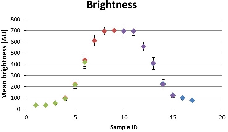
The effect of the annealing process can be investigated using flat angle illumination and detect the reflected light. The intensity of this reflected light is shown to be in correlation to the layer quality and has a peak at the optimal energy density.
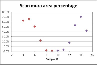
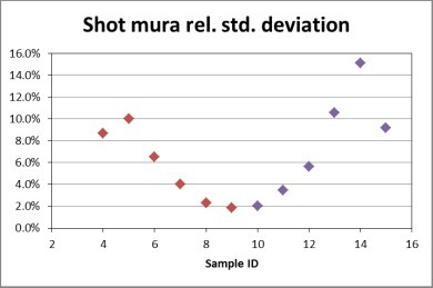
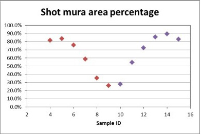
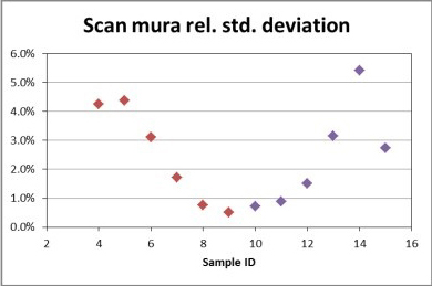
Possible sources of p-Si layer inhomogeneities and defects are the laser optical system and the scanning system instability. Both can be investigated by the Line Mura metrology by detecting their visible marks on the thin film using state of the art image processing techniques: they are shown as Shot Mura and Scan Mura on the Line Mura images. The strength and the density (area percentage) of these mura effects can be determined.
FEATURES
- Accurate determination of optimal energy density
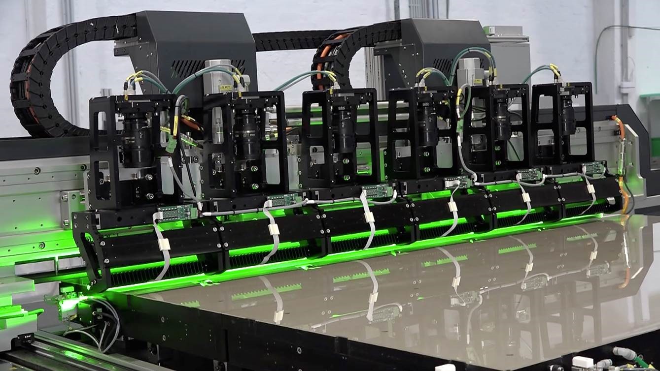
- Capable to mount multiple Line Mura measurement head for faster tact time
- Combination of optical and electrical measurement for more precise judgement
- Automatic judgement of each chip (device) based on judgement criteria set in recipe
Product Line
FPT
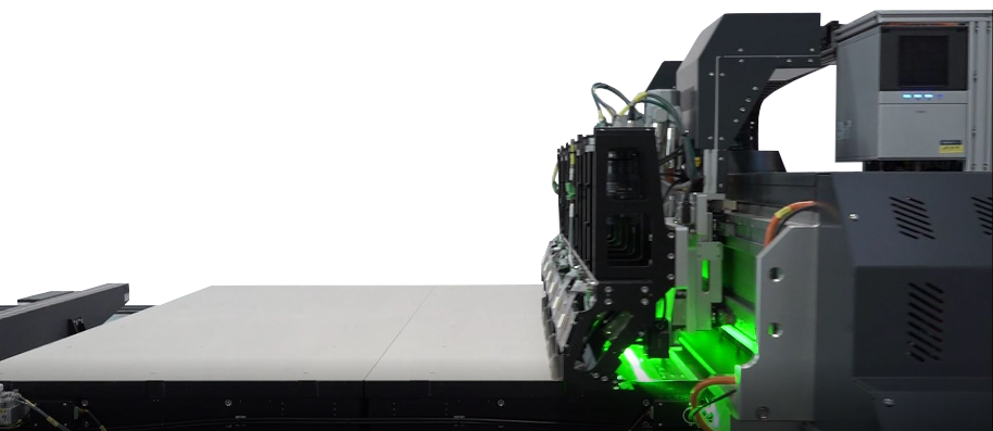
FPT- series are dedicated for flat panel testing and characterization. The products are designed to characterize LCD and AMOLED TFT panels up to GEN 8.5. It is capable to combine several measurement probes into one platform, providing high precision measurements over the entire surface of flat panels with high accuracy and fast motorization stage and weight capacity.
Products

FPT
FPT can be equipped with:
- Spectroscopic ellipsometry
- Spectroscopic reflectometry
- Imaging Spectroscopic reflectometry
- Line mura detection - Chip quality
- Microwave Photoconductive Response - Chip Quality
- Four point probe & six point probe
- Contact angle measurement
- Raman crystallinity
Optical thickness and refractive index of multilayered oxide and semiconductor structures can be determined by spectroscopic ellipsometery at different process steps. The quality of the ELA process can also be monitored by measuring crystallinity, u-PCR and line mura density. Contact angle, stress and resistivity measurements are also available.
The hardware and software are fully controlled by SEMILAB from the design to the integrated software communication with the fab.