


Application
ELA PROCESS CHARACTERIZATION (LTPS)
Excimer Laser Annealing (ELA) is the key process parameter in Low Temperate Silicon (LTPS) layer manufacturing: ELA determines many important final parameters of the layer and finally of the device: crystallinity, mobility, etc. Semilab developed a combination of metrologies which can easily determines the Optimal Energy Density (OED). This combination is capable to distinguish the properties of two LTPS samples which were annealed with very similar annealing parameters. Using this feature fine tuning of ELA process is easy and fast and does not require any macro inspection with human decision.
Furthermore using our contact 6pp the sheet resistance can be determined as well.
Technology
SHEET RESISTANCE MEASUREMENT
The combination of the ion implant process and the process to anneal implants is usually monitored by measuring the sheet resistance of the implanted layer. The sheet resistance varies with dose, energy, and the amount of implanted species that has become electrically active. It is the sheet resistance that ultimately determines the device performance. Thus, measuring sheet resistance is an excellent way to monitor everything associated with an implant process.
The basic idea of the JPV method is the light excitation of the np or pn layer structure, and the pick-up of the resulting junction photovoltage by a capacitive probe. The detected potential is determined by the sheet resistance of the implanted layer, capacitance of junction and resistance through over the diode.
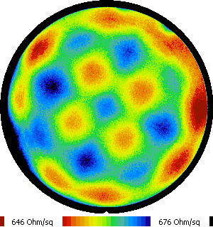
Figure 2. Sheet resistance measurement (lower range)
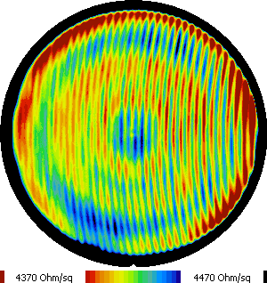
Figure 3. Sheet resistance measurement (higher range)
Semilab offers JPV technology to make non-contact, high resolution fast maps of sheet resistance.
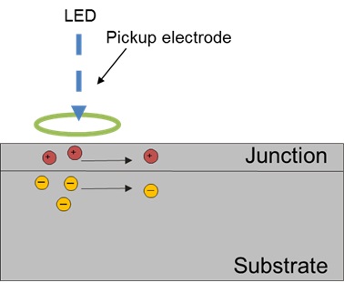
Figure 4. Measurement theory
MEASUREMENT THEORY:
The sample is illuminated by chopped LED light, which generates electrons and holes in the substrate layer. The generated charge carriers diffuse to the junction and the electric field located in the junction separates them. The result of the separation is the change in the junction voltage. This voltage change spread laterally in the implanted layer and the attenuation depends on the sheet resistance, junction capacitance, resistance of the junction and chopping frequency of the LED.
The potential change is detected by a capacitive sensor in order to evaluate the JPV signal, as a function of the frequency of the emitted light.
Based on the evaluation, the sheet resistance (Rs), capacitance of junction (Cd) and the resistance of the diode (Rd) can be calculated.
The junction leakage current is directly connected to the Rd by the following equation:
I_L=kt/q/R_d
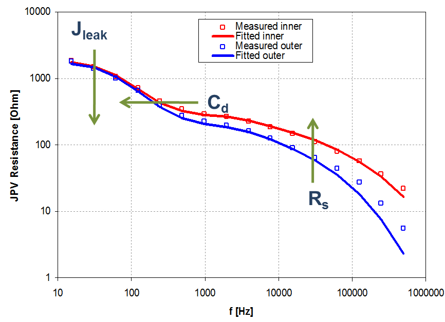
Figure 5. The detected potential is determined by Rs, Cd, Rd and frequency
FEATURES
- Non-contact, non-destructive
- No probe conditioning
- No sample preparation needed
- Works through oxide or coating
- High resolution mapping capability
- Fast mapping
- Good repeatability
Product Line
FPT
Light sources: monochromatic LED, wavelength can be 470 nm, 520 nm, 740 nm and 970 nm (depending on junction depth)
Lateral resolution: 1 mm
Resolution in X-Y mapping: 1, 2, 4, 8 and 16 mm spatial resolution, or single point measurements at predefined points (up to 50)
Samples: np or pn structure (diffused or implanted USJ)
Products

FPT
FPT can be equipped with:
- Spectroscopic ellipsometry
- Spectroscopic reflectometry
- Imaging Spectroscopic reflectometry
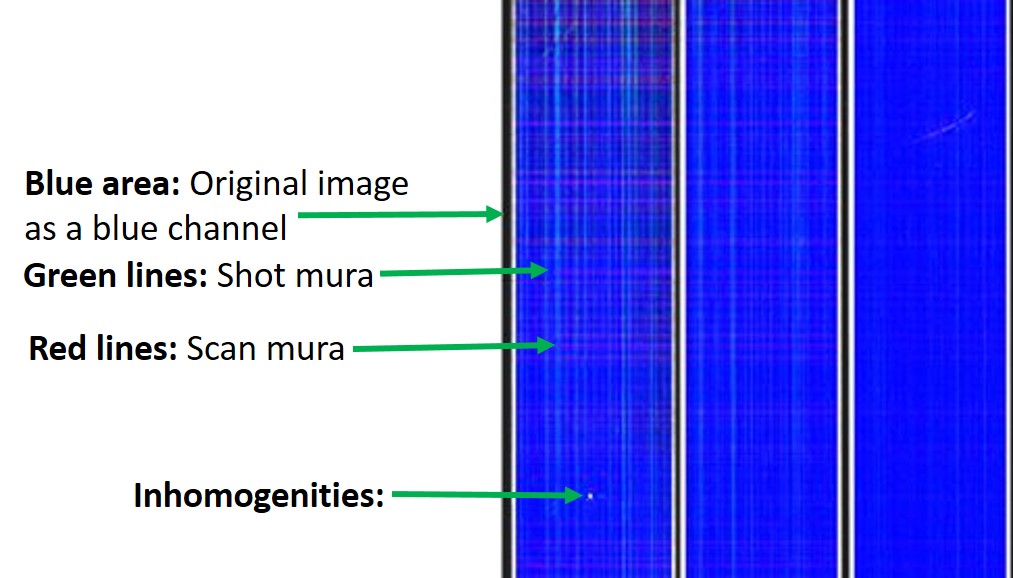
- Line mura detection - Chip quality
- Microwave Photoconductive Response - Chip Quality
- Four point probe & six point probe
- Contact angle measurement
- Raman crystallinity
Optical thickness and refractive index of multilayered oxide and semiconductor structures can be determined by spectroscopic ellipsometery at different process steps. The quality of the ELA process can also be monitored by measuring crystallinity, u-PCR and line mura density. Contact angle, stress and resistivity measurements are also available.
The hardware and software are fully controlled by SEMILAB from the design to the integrated software communication with the fab.
Request Info