


Product release - New automated Semilab AFM metrology system with state-of-the-art combination of surface characterization methods
07.09.2023
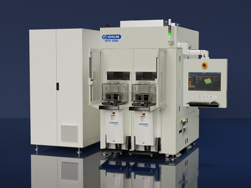
We are pleased to release the Semilab AFM-3000, the automated Semilab Atomic Force Microscope system.
The newest AFM system of Semilab provide high-resolution measurements with sub-atomic precision and extremely low noise level, which enables consistent and highly reproducible roughness characterization for the quality control of up to 12” semiconductor wafers.
Silicon and compound wafer makers may also benefit from the AFM systems’ advanced defect review capability, as high-resolution AFM measurement is combined with micro-particle inspection metrology for immediate determination of the real position and 3D structure of the detected defects.
Semilab’s automated AFM systems fulfill industrial standards in micro and nano-topology measurement, based on the high-resolution 3D surface profiling technique of atomic force microscopy.
With the ultimate unification of cutting-edge technology and the decades-long know-how, Semilab AFM systems allow a stable and accurate performance in a widely customizable, user-friendly environment, and with that, they provide real, detailed 3D sample surface information and precise defect localization.
Technology background
As the size of the devices continues to decrease, and their structures are becoming more complex, even the smaller defects can impact the performance of the device to be manufactured. Due to this trend, manufacturing processes require sub-atomic precision and there is also a special demand on the quality control of the wafers’ surface in the nanometer range.
Therefore, roughness characterization and defect detection of the semiconductor wafers in nanoscale is essential for Si, SiC, GaN or μLED wafer makers.
Applications
- Roughness measurements
- CMP process control
- Defect detection by light scattering method (µPIT) and characterization
Benefits
AFM systems’ novel hardware and customizable software enable consistent quality control of semiconductor wafers:
- Improved quality inspection:
- Roughness measurement of silicon samples after CMP
- Defect inspection on micro- and nanoscale, real 3D information
- µPIT: Enables the precise localization of defects by light scattering method based on imported KLARF files
- Customizable software
- Full Wafer AFM Profilometer Mode: speed/scan area optimalisation
- Pattern recognition
- Wafer contour meter for repeatable and precise alignment
- KLARF defect file import
The system fulfills industrial standards with its modern platform:
- Manual & automated systems are available for handling wafers up to 300 mm sizes
- Low noise platform – high performance acoustic and vibration isolation
- 10.000x tip exchange without failure
Semilab AFM-3000 system is essential FOR ALL YOUR SURFACE MEASUREMENT NEEDS!