


Application
SI INGOT/ BLOCK TESTING
The quality of the silicon crystal determines the maximum achievable conversion efficiency of the final photovoltaic device. Thus, the quality control of the as-grown Si crystals is crucial to stabilize the manufacturing of modern Si solar cells. Semilab offers various solutions to control all the important material parameters in both multi- and monocrystalline silicon ingots.
Resistivity of the mono and multicrystalline ingots is tested by using eddy current sensor, integrated into various system platforms.
Metallic contamination and extended crystal defects are detected by using different versions of PhotoConductance Decay and Photoluminescence methods.
Finally, our Infrared Imaging system localizes the larger precipitations in the crystal in order to prevent the failures in the wire sawing process.
Technology
µ-PCD CARRIER LIFETIME FOR MULTI-SI
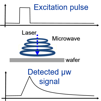
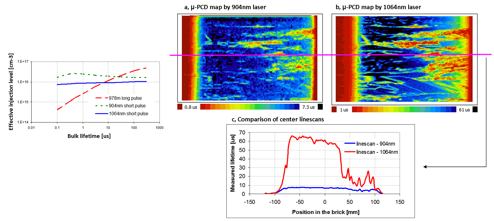
Microwave PhotoConductance Decay (µ-PCD) technique based carrier lifetime mapping is a common way characterize the electrical quality of raw silicon material for photovoltaic applications. It is applied for the qualification of bulk Si materials. During the material production one of the main function of the µ-PCD measurement is to define the edge of the strongly contaminated top and bottom parts of the silicon bricks. Quality control of the good quality middle region has an increasing importance (e.g. for the production of high performance multi, HPM silicon). Thus, a reliable and well understood bulk lifetime characterization method is required for this purpose. The traditional µ-PCD configuration (with 904nm excitation laser) provides proper information about the recombination lifetime in the “red-zone”, however in the middle zone the measurable decay time is limited at ~10µs as an upper whereas the real bulk lifetime might be several hundreds of microseconds. This detectable “effective lifetime” can be increased significantly by changing the properties of the laser source used for the excess carrier generation during the µ-PCD measurement. Based on simulation and experimental results an optimized µ-PCD configuration is suggested for this application which applies:
- 1064nm short pulse laser
- Standard µ-PCD antenna
Advantages of this configuration:
- Laser upgrade in WT-2000 system family is possible for better multi-crystalline Silicon ingot characterization
- Relatively stable injection level can be achieved on the entire Si brick. It makes the analysis of the results simpler.
Effect of excitation laser properties to injection level is demonstrated on the below example. Using short pulse lasers a relatively stable injection level can be achieved on the entire Si brick. It makes the analysis of the results simpler.
FEATURES
- Short pulse laser increases the measurable lifetime
- Increased sensitivity to any defects in bulk
- Enabled to study the injection level during the measurement
- Stable effective injection level of the measurement
Product Line
WT
The WT product line is a powerful measurement platform for performing many different semiconductor material characterization measurements. The base system includes all the overhead functions necessary to perform characterization measurements, including power supplies, computer and operating software, XY measurement stage, etc. The WT-2000 is typically used to make maps, where the wafer is scanned at a programmable raster. Each system is configured to the user’s requirements by adding treatment and measurement capabilities.
Products

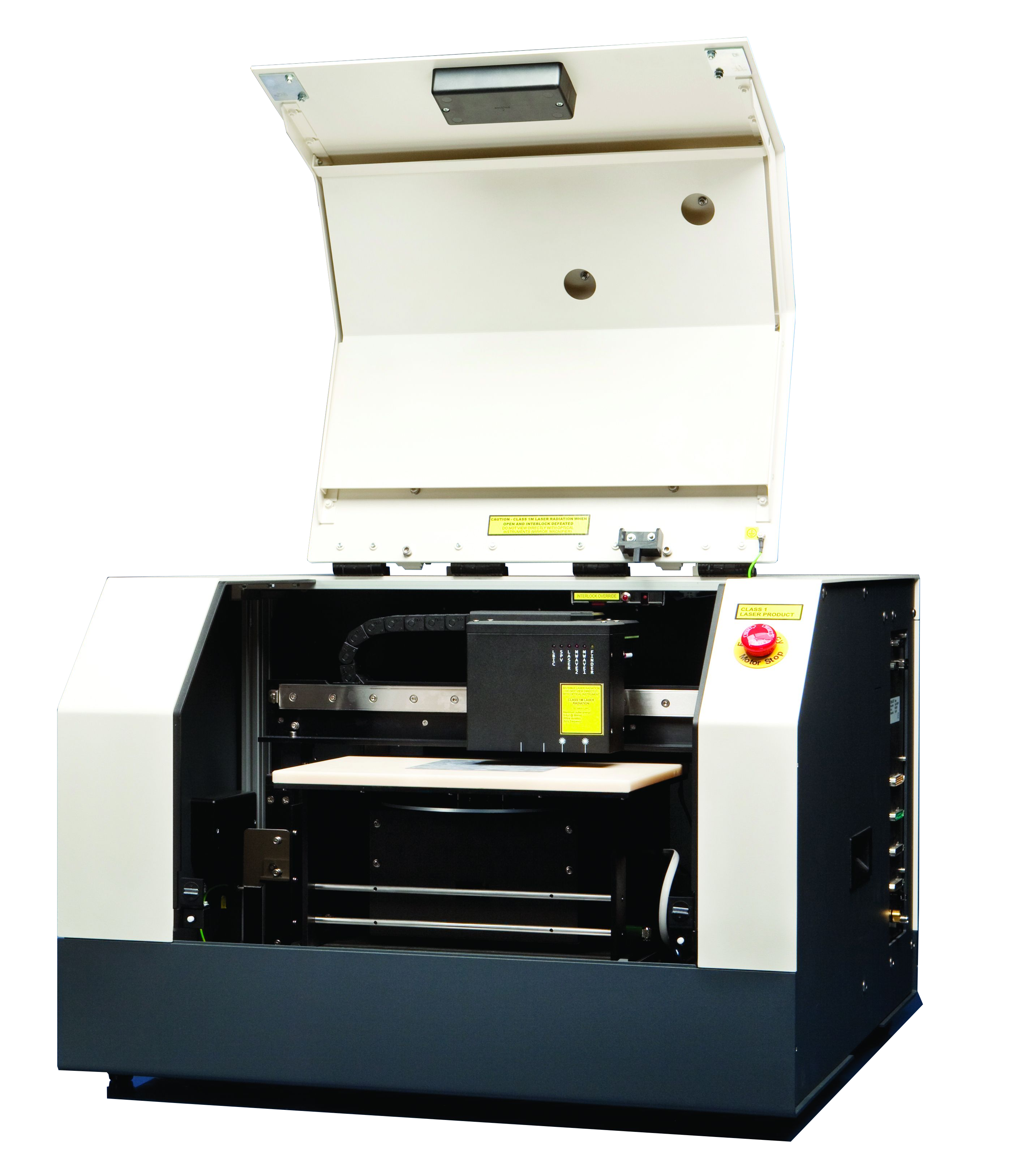
WT-2010D
The WT-2000D is a complete measurement tool for monitoring quality of silicon blocks by measuring Carrier recombination lifetime and resistivity. The system provides fast, non-contact measurements (single-point, line scans and/or maps) on silicon blocks in size up to 210x210x500 mm. It has manual and automatic measurement modes and manual block loading capabilities.
Carrier recombination lifetime is a primary quality control parameter for multi-crystalline silicon blocks. The measurement is based on µ-PCD technique.
Resistivity is measured based on eddy current technique.
Request Info