


Application
SI WAFER SORTING
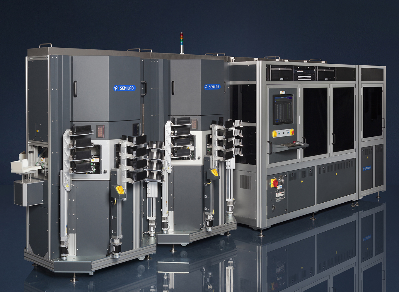
Sorter applications provide advanced multiparameter wafer inspection with integrated high speed sorting for quality control of production PV wafers. Owing to wide range automation module portfolio and flexible combined Semilab’s metrology modules, all customer can find perfect configuration what fulfil their production expectations.
Application area:
- Outgoing wafer inspection for wafer manufacturers
- Incoming as-cut wafer inspection for solar cell manufacturers
Sorter purpose
- Eliminating damaged wafers from further process
- Eliminating high thickness variation wafers (TTV, saw mark)
- Sorting of potentially weak wafers (microcracks) which could break in subsequent process steps
- Sorting based on resistivity, and lifetime values
- Sorting of wafers with dislocations, high contamination and vacancy density
- Wafer input: loading from cassettes or stack
- Wafer output: Sorting in different user-defined classes, collection in coin stacks
- High throughput
Technology
GEOMETRY INSPECTION
2D Geometry Inspection of the wafers is served by SHP module of the sorters. It is on-the-fly process where the wafer passes through between the camera and the flashing panel. 2D matrix camera takes the silhouette image of the moving wafer. Edge-detection algorithms search the side-edges of the wafer. The found edge points are transformed to mm coordinates. Several distortion effects are eliminated during the image processing (e.g. pillow effect).
On the fly wafer measurement of the following parameters:
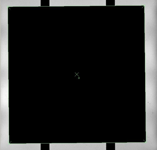 Example image of SHP
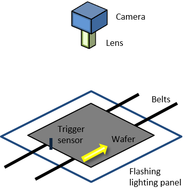
Imaging and image processing method is based on signal detection of the fixed camera generated by flashing lighting panel. The wafer passes through between the camera and the flashing panel. Capacitive sensor detects the incoming wafers and the controller circuit is timing the illumination panel flash and starts the image acquisition in a proper time. 2D matrix camera takes the silhouette image of the moving wafer additionally Edge-detection algorithms searches the side-edges of the wafer. The found edge points are transformed to mm coordinates.
Several distortion effects are eliminated during the image processing (e.g. pillow effect).
After transformation, the following steps are done:
- Line fitting on the edges
- Circle fitting on the chamfer
- Calculation of the geometric information
FEATURES
Product Line
PVS
The PVS product line provides advanced multi-parameter wafer inspection with integrated high speed sorting for quality control of production wafers. It eliminates imperfect substrates, maximize cell line output and ensures optimized efficiency.
It combines high reliability wafer handling with Semilab’s industry leading PV metrology, to provide a turnkey solution for sorting of incoming wafers. This is backed by direct expert support from the OEM metrology manufacturer, through our worldwide network of branch offices.
Products
PVS-5100
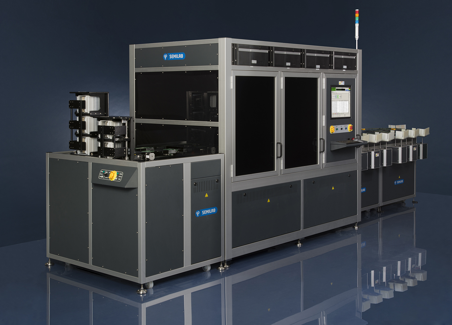
PVS-5100 is a high throughput, field proven PV Wafer Inspection and Sorting System.
It combines high reliability wafer handling with Semilab’s industry leading PV metrology, to provide a turnkey solution for sorting of incoming wafers. This is backed by direct expert support from the OEM metrology manufacturer, through our worldwide network of branch offices.
Loaders
- PVLS-5400 Automated stack loader with 3 position pick-and-place system. Up to 2400 pcs buffered wafer in 12 pcs carrier.
- PVLC-3600* Automated cassette loaders for 25/50/100 slot cassettes
- PVLC-3600-AL Fully automated production line loader for 100 slot cassettes
Metrologies
- PLI-101/3 Photoluminescence imaging
- WML-1 Minority carrier lifetime measurement
- SHP-200 2D measurement
- MCI-150 Micro crack inspection
- WSI-120 Surface chipping and contamination inspection
- TTR-300 Thickness, resistivity measurement
- TTR-300 Saw mark Inspection
Unloaders
- PVULS-5406T High speed stack unloader with 6 bin
- PVULS-5407T High speed multilevel stack unloader with 7 bin
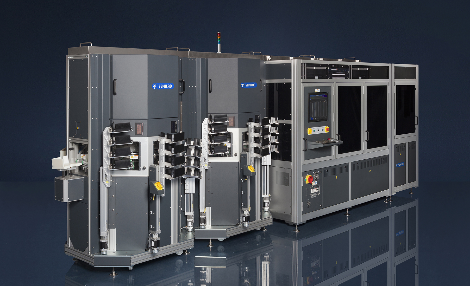
PVS-6000
PVS-6000 is a High Speed, field proven PV Wafer Inspection and Sorting System with 5400 wafer per hour throughput. It combines high reliability wafer handling with Semilab’s industry leading PV metrology, to provide a turnkey solution for sorting of incoming wafers. This is backed by direct expert support from the OEM metrology manufacturer, through our worldwide network of branch offices.
Loaders:
- PVLS-5400 Automated stack loader with 3 position pick-and-place system. Up to 2400 pcs buffered wafer in 12 pcs carrier.
- PVLC-3600 Automated cassette loaders for 25/50/100 slot cassettes
- PVLC-3600-AL Fully automated production line loader for 100 slot cassettes
Metrologies:
- PLI-101/3 Photoluminescence imaging
- WML-1 Minority carrier lifetime measurement
- SHP-200 2D measurement
- MCI-150 Micro crack inspection
- WSI-120 Surface chipping and contamination inspection
- TTR-300 Thickness, resistivity measurement
- TTR-300 Sawmark Inspection
Unloaders:
- PVULS-5406T High speed stack unloader with 6 bin
- PVULS-5407T High speed multilevel stack unloader with 7 bin