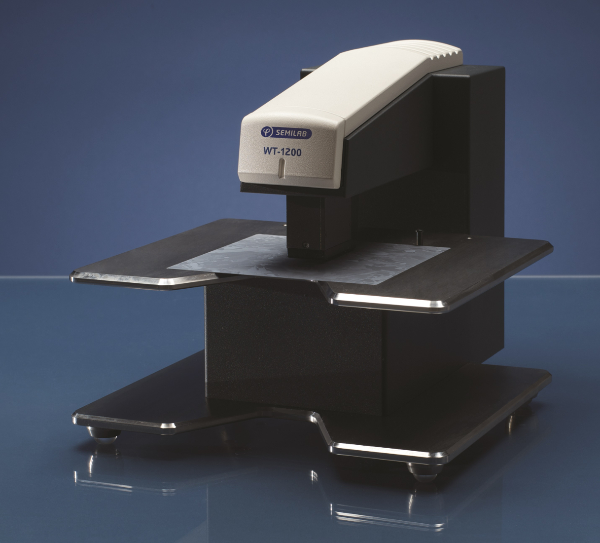
WT-1200 & WT-1200B
Low Cost, Non-Contact Single-Point Measurement in Silicon
Both WT-1200 and WT-1200B provide fast, non-contact carrier lifetime measurement method that is capable of characterizing silicon material in each process step of solar cell manufacturing.
WT-1200 is designed to measure wafers from as-cut wafer to the finished solar cell. WT-1200B is a model for block measurements.
Features and System specifications:
- No need for access to back side of the wafer
- Fully automatic operation and data evaluation
- Measurement selectable at any position on the wafer
- Measurement of mono- and multi-crystalline material
- Patented chemical surface passivation option available for wafers
- Wafers can be measured after each process step of solar cell manufacturing:
- Incoming as-cut wafer
- Diffused wafers (with or without phosphorous glass)
- Nitride coated wafers
- Metallized wafers
- Finished solar cells


