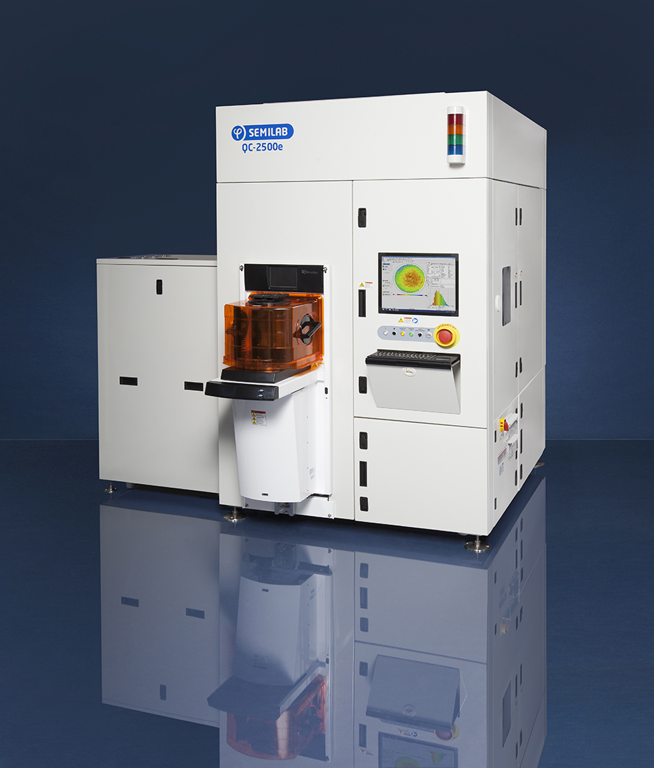
QC-series
Semilab’s QC platforms (Near Surface Doping Mappers) for epitaxial monitoring are the only non-contact, non-destructive, high throughput systems that can reliably map near surface doping on process wafers.
Features:
- Integrated universal (for both p- and n-type) UV/Corona pre-treatment with improved and optimized UV oxidation for up-to 300 mm wafers and accurate feedback loop controlled corona charging technique with new mechanical and electronics design and new corona system.
- New sensor design insensitive to wafer/chuck flatness.
- Rapidity of even full wafer mapping measurements ensures an impressive throughput and the ability to monitor and control the epitaxial process
- Improved new software has multiple benefits, such as: highly configurable, multitasking, real-time data monitoring, simplified recipe generation, job queuing and fully 300mm SECS/GEM complaint.
- Wafer motion stage with precise positioning
- Detects problems that may escape other metrology techniques, because of the strong surface sensitivity
- Qualifies Epi layer within the critical device region of IC
- Provides near-surface carrier lifetime as an indicator of wafer contamination
- Fast full wafer mapping capability
- Measures all doping combinations: n/p, n/n, p/n, p/p
| QC-2200e | QC-2500e | QC-3000e | |
|---|---|---|---|
| Wafer size | up to 200 mm |
up to 300 mm |
up to 300 mm |
| Platform | Full hand-off automated | Full hand-off automated | Full hand-off automated |
| Load port | 1 loadport / FOUP | 1 loadport / FOUP | 2 loadports / FOUP |
|
Primary applications:
|
|
|
| Equipments: | Measurement parameters: | Measurable wafer types: |
|
|
|
Request Info


