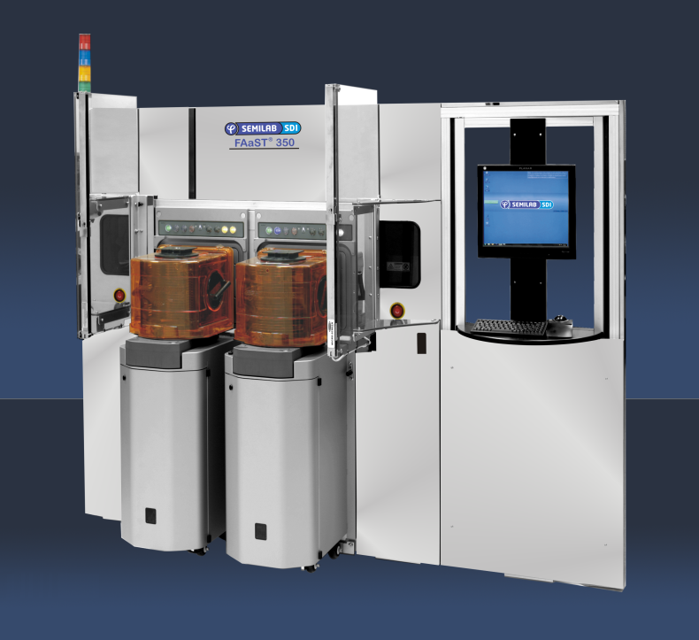
FAaST 350 C-V / I-V
The FAaST 350 C-V / I-V system applies Semilab SDI’s advanced C-V / I-V measurements based on patented corona-Kelvin methods to non-contact imaging of dielectrics and interface properties. This workhorse platform is designed with automated wafer handling from dual FOUP Loadport loading stations fully capable of supporting in-line measurements in the most demanding high-volume manufacturing environment.
Features and System specifications:
- Automatic robotic wafer handling
- Dual FOUP Loadport; optional configuration with single Loadport or including Versaport
- Full wafer Non-Visual Defect (NVD) Inspection and Plasma Damage Monitoring using Surface Voltage FAST Mapping mode
- Automatic programmable sites or contour mapping of dielectric properties including:
- Dielectric Capacitance (CD) and Thickness (EOT)
- Dielectric Leakage Current (I-V)
- Flatband Voltage (Vfb)
- Interface Trap Density (Dit)
- Interface Trapped Charge (Qit)
- Semiconductor Surface Barrier (Vsb)
- Oxide Total Charge (Qtot)
- Mobile Ionic Charge (Qm), among others
- FAaST software package; including Measurement, Recipe Writing and Data Viewing applications
- Suitable for measurement on: semiconductors (e.g. Si, SiGe, InGaAs, SiC, GaN) with high-k and low-k dielectric films (e.g. SiO2, SiNx, Al2O3, HfO2 ; mixed dielectrics and dielectric film stacks)
- Default configuration for 300mm wafers; with option for 200mm/300mm bridge configuration
- Line Conditioner with flexible compatibility
- Compatible for configuration with other Semilab SDI FAaST tool measurement technologies
- Additional available options include: Mini-environment, 300mm Semi compliant Automation, Seismic brackets, wafer OCR, RFID, cassette barcode reader, 1000V Vcpd measurement range


