


Application
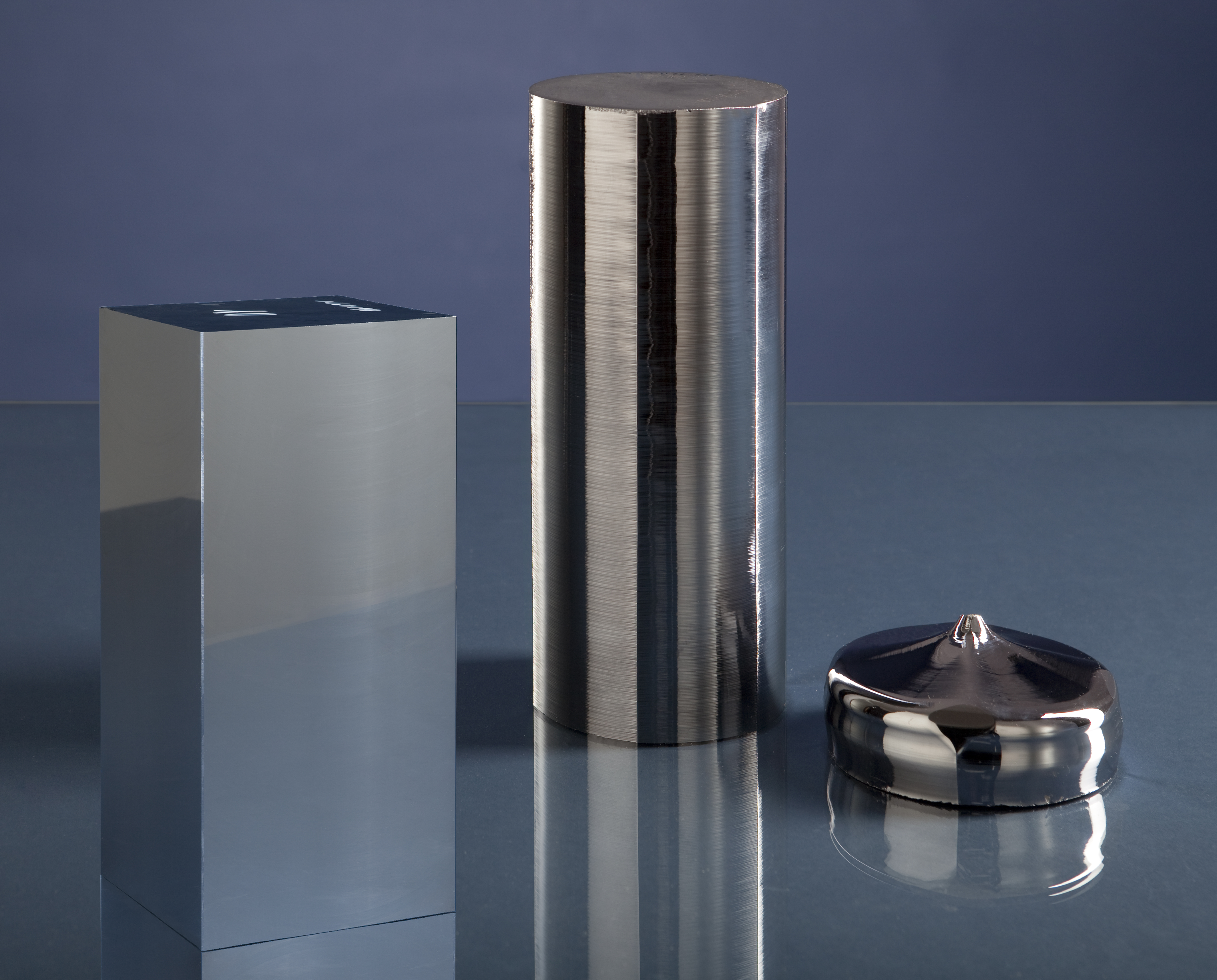
SI INGOT/ BLOCK TESTING
The quality of the silicon crystal determines the maximum achievable conversion efficiency of the final photovoltaic device. Thus, the quality control of the as-grown Si crystals is crucial to stabilize the manufacturing of modern Si solar cells. Semilab offers various solutions to control all the important material parameters in both multi- and monocrystalline silicon ingots.
Resistivity of the mono and multicrystalline ingots is tested by using eddy current sensor, integrated into various system platforms.
Metallic contamination and extended crystal defects are detected by using different versions of PhotoConductance Decay and Photoluminescence methods.
Finally, our Infrared Imaging system localizes the larger precipitations in the crystal in order to prevent the failures in the wire sawing process.
Technology
BLOCKS' PHOTOLUMINESCENCE IMAGING
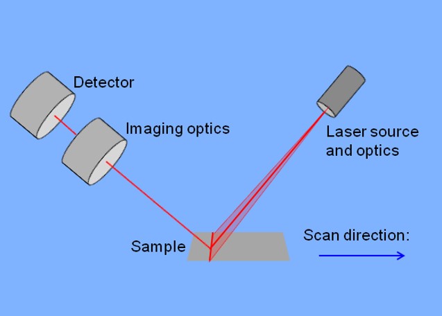
Photoluminescent Imaging is an excellent method for monitoring of multicrystalline, monocast or monocrystalline blocks. During the measurement, the laser illuminates the silicon block and the generated photoluminescent signal is detected by an IR camera. The illumination effects the recombination of charge carriers. If not, the defects are present and there is a chance of radiative recombination. During the radiative recombination, a photon is emitted which can be detected by an IR camera. PL intensity is inversely proportional to defect density and impurity concentration.
Benefits:
- High quality fast imaging even for as cut blocks
- Block sides lifetime mapping using lifetime calibration method
- Flexible classification according to the requirements
- Accurate tool-to-tool matching capability
- Flexible configurability of measurement equipments from stand-alone to integration in fully automated systems
Facts
- Industry is moving toward more automated factories
- Industry requirement for multipurpose control station:
- Reduced sample handling and transport time
- Facility integration capability and robot loading support
- Integrated quality control
Measurement examples
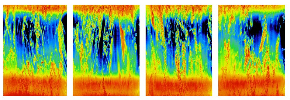
PLB measurement example - PL images
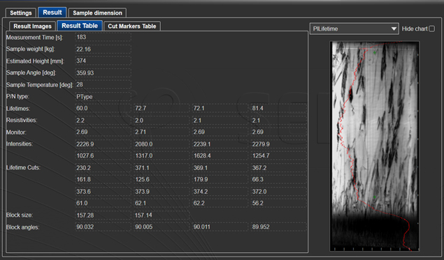
PLB measurement result example
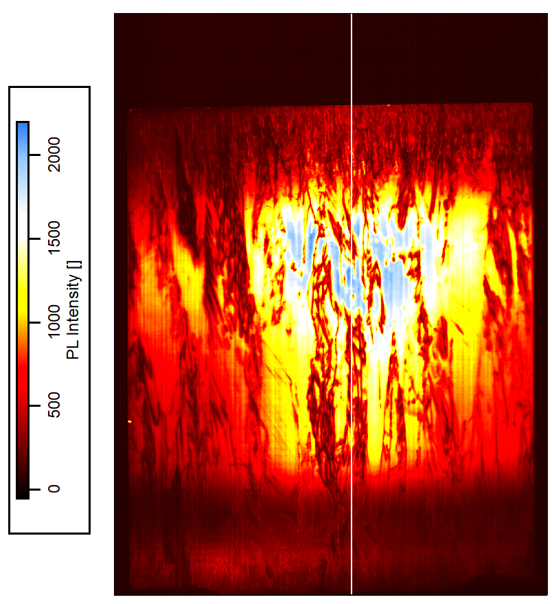
![]()
PL image with the position of measured µ-PCD line (left), comparison of PL image pixel intensity and µ-PCD value at the same area (right)
FEATURES
- Photoluminescence image on polished and as-cut blocks
- On the fly lifetime map from µ-PCD calibrated PL image
- Applicable for R&D usage
- Quality description by calibrated lifetime maps and customizable classification parameters
Product Line
PLB
Block photoluminescence imaging system for wafer and cell inspection is a fast and reliable solution for non-destructive quality measurement of silicon blocks.
- Supports more cost-effective production by providing material quality control of blocks.
- High resolution and high throughput bulk-lifetime mapping based on Photoluminescence imaging
- High versatility: 9 measurement types in one station
- Enable brick autoloading through fab automation (ease of integration)
Products

PLB-55 Photoluminescence Silicon Block Imaging System
PLB is fast, non-contact, easy-to-use system to detect defects and impurity concentration in silicon blocks for photovoltaic application.
Features and System specifications:
Ingot Imaging system:
- Photoluminescence lifetime measurement - mapping for all 4 sides
- Max block size: 159×159×500 mm
- Block type: polished or non-polished block
- IR transition based inspection
- Built in integrated μ-PCD lifetime measurement with 1 probe for in-situ calibration - 1 line scan per side and lifetime calibration of the entire PL image.
- Block size determination with built Omron optical sensors
- Built in eddy head for resistivity measurement 1 line scan per side
- Built in P/N tester for conductivity type determination 1 line scan per side.
- Weight measurement (Max. 50 kg, 20 g accuracy)
Additional Measurements:
- Resistivity measurement with eddy head
- Lifetime measurement with μ-PCD head
- Temperature measurement with pyro sensor
- PN conductivity type measurement
- Block weight measurement
- Block size measurement
- Block angle measurement
Software evaluation:
- Calculated lifetime map
- Determination of the cutting line based on lifetime
- Determination of the cutting line based on resistivity
- Defect area percentage
- Colored images
- Export data to Excel
Options:
- High resolution images (transmission, PL)
- Fully automated robot support
- Block marker and printing
- G-code for CNC machines
- MES
- Slug measurement for R&D
- Language options: English, Chinese, Hungarian, for other, please contact us