


Application
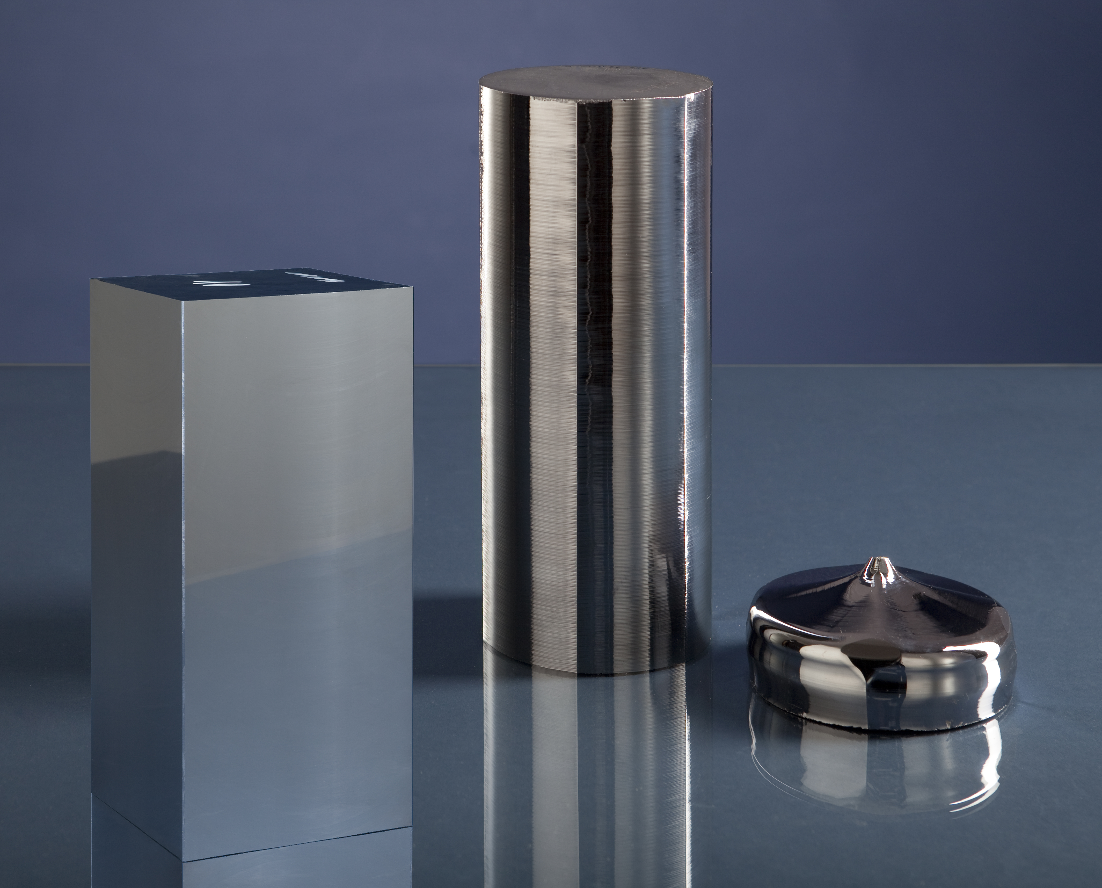
SI INGOT/ BLOCK TESTING
The quality of the silicon crystal determines the maximum achievable conversion efficiency of the final photovoltaic device. Thus, the quality control of the as-grown Si crystals is crucial to stabilize the manufacturing of modern Si solar cells. Semilab offers various solutions to control all the important material parameters in both multi- and monocrystalline silicon ingots.
Resistivity of the mono and multicrystalline ingots is tested by using eddy current sensor, integrated into various system platforms.
Metallic contamination and extended crystal defects are detected by using different versions of PhotoConductance Decay and Photoluminescence methods.
Finally, our Infrared Imaging system localizes the larger precipitations in the crystal in order to prevent the failures in the wire sawing process.
Technology
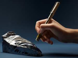
P/N TYPE DETERMINATION
The operation of the P/N Tester is based on the SPV (Surface Photovoltage) technique. The excitation is represented by chopped light, which periodically generates free carriers (electron-hole pairs) in large concentration. A high sensitivity probe is capacitively coupled to the sample close to the sample surface. The surface potential barrier of the sample is periodically changed by the chopped light and can be measured by the p/n probe. When the light is on, the sample is near to the flat-band condition. When the light is off, the sample has a larger surface potential barrier. The signal stands for the difference between the potential values measured during the bright and the dark periods of the excitation. Since the sign of the signal depends on the conduction type of the sample, this method can be used for conduction type determination.
The technique has certain limitations:
- Thermal donors (oxygen) can yield false measurements
- Oxide charge on the surface can also adversely affect the measurement
- The measurement result on p-n or n-p structured wafers depends on the layer thickness (The P/N Tester measures either the substrate or the layer, depending on the layer thickness.)
- Residue of passivating materials, acids, and other active chemicals can adversely affect the measurement as well.
- It is difficult to measure as-cut samples in some cases, when the damaged layer is much thicker than the penetration depth of the light used by the P/N Tester
FEATURES
- Easy to use
- Non-contact testing
- Portable tools
Product Line
PN
PN tools are off-line, discrete point measurements suitable for feedstock or reclaim material. The easy handling is guaranteed by handheld, portable and table-top constructions.
Products

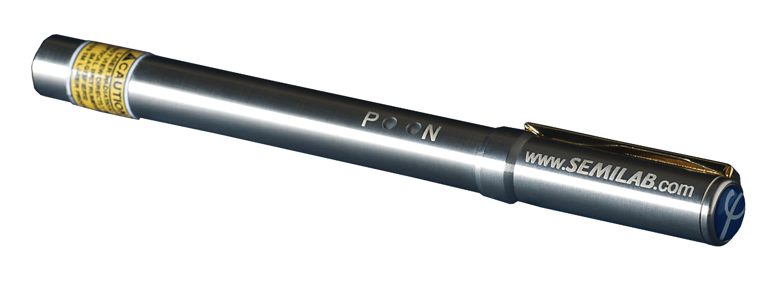
PN-100
PN-100 is a fast, easy-to-use, non-contact tool for determining conductivity type (p or n) of the semiconductor materials.
Features and System specifications:
- Type determination of silicon blocks and wafers including single- or multicrystalline material as well as bare and oxidized wafers
- Measurement time: 0.5 s
- Result display:
- Red LED = P-type
- Green LED = N-type
- Resistivity range: 20 mΩcm to 3000 Ωcm
- Measurement spot: diameter depends on the distance: ~10-20 mm
- Excitation depth: ~3 μm
- Measuring distance depends on the resistivity and surface: e.g. for 10 Ωcm material with polished surface ~20 mm
- Number of measurements without exchanging the battery: ~10.000