


Application
SI INGOT/ BLOCK TESTING
The quality of the silicon crystal determines the maximum achievable conversion efficiency of the final photovoltaic device. Thus, the quality control of the as-grown Si crystals is crucial to stabilize the manufacturing of modern Si solar cells. Semilab offers various solutions to control all the important material parameters in both multi- and monocrystalline silicon ingots.
Resistivity of the mono and multicrystalline ingots is tested by using eddy current sensor, integrated into various system platforms.
Metallic contamination and extended crystal defects are detected by using different versions of PhotoConductance Decay and Photoluminescence methods.
Finally, our Infrared Imaging system localizes the larger precipitations in the crystal in order to prevent the failures in the wire sawing process.
Technology
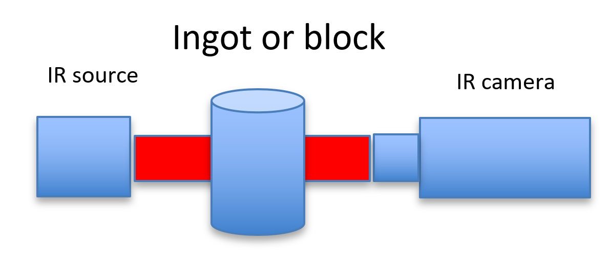
INFRARED BLOCK IMAGING
Infrared Imaging technology is a powerful method for inspection of Si blocks/ ingots during the manufacturing process. With Infrared Imaging it is possible to avoid the undesirable effect of inclusions, slip-lines, thermally induced internal stress and other defects degrading the quality of solar wafers. Identification and localization of Carbid and Nitrid inclusions lengthens the lifetime of sawing lines considerably, therefore, reducing maintenance requirements.
The high intensity IR source illuminates the block or ingot with lower photon energy than the band gap of silicon. Identification and localization of Carbid and Nitrid inclusions lengthens the lifetime of sawing lines considerably, therefore, reducing maintenance requirements. The image of the light - which goes through the sample - is recorded by a short wavelength IR line scan camera.
Detectable defects in Si blocks/ingots:
- Cracks, internal propagation of cracks
- Voids
- Inclusions - precipitates in the block/ingot, usually silicon carbide (SiC) and silicon nitride (Si3N4)
- Microcrystalline silicon - may form due to disturbances in the melt silicon. This may degrade the efficiency of solar cells.
- Slip lines
- Thermally induced internal stress
FEATURES
- Non-contact, non-destructive technology
- Four side block scanning provides the exact position of the defects and contaminations
- Fast scanning
- Internal stress and slip line zone determination
Product Line
PLB
PLB product line consists of ideal systems for non-contact determination of defects and impurity concentration in polished or unpolished silicon blocks or ingots for photovoltaic application.
The PLB system includes either the photoluminescence lifetime measurement with µ-PCD or IR transmission measurement.
Products

PLB-55i Silicon Block Scanner
This is a fast, non-contact, easy-to-use system to detect defects in silicon blocks for photovoltaic application.
Types of detectable defects:
- Crack
- Void
- Inclusion
- Growth band
Features and System specifications:
- Cut position is determined with 0.1 mm accuracy
- Integrated motor driven rotary stage for all 4 side measurement
- All 4 sides are measured automatically
- Automatic evaluation software
- Ingot type: Polished, non-polished
- Max. ingot size: 500×210×210 mm
- Operation: Automatic or manual
- Real time spot detection: Included
- 3D Visualization: Included
- Automatic evaluation: Included
- Automatic software evaluation with block images

PLB-55 Photoluminescence Silicon Block Imaging System
PLB is fast, non-contact, easy-to-use system to detect defects and impurity concentration in silicon blocks for photovoltaic application.
Features and System specifications:
Ingot Imaging system:
- Photoluminescence lifetime measurement - mapping for all 4 sides
- Max block size: 159×159×500 mm
- Block type: polished or non-polished block
- IR transition based inspection
- Built in integrated μ-PCD lifetime measurement with 1 probe for in-situ calibration - 1 line scan per side and lifetime calibration of the entire PL image.
- Block size determination with built Omron optical sensors
- Built in eddy head for resistivity measurement 1 line scan per side
- Built in P/N tester for conductivity type determination 1 line scan per side.
- Weight measurement (Max. 50 kg, 20 g accuracy)
Additional Measurements:
- Resistivity measurement with eddy head
- Lifetime measurement with μ-PCD head
- Temperature measurement with pyro sensor
- PN conductivity type measurement
- Block weight measurement
- Block size measurement
- Block angle measurement
Software evaluation:
- Calculated lifetime map
- Determination of the cutting line based on lifetime
- Determination of the cutting line based on resistivity
- Defect area percentage
- Colored images
- Export data to Excel
Options:
- High resolution images (transmission, PL)
- Fully automated robot support
- Block marker and printing
- G-code for CNC machines
- MES
- Slug measurement for R&D
- Language options: English, Chinese, Hungarian, for other, please contact us

PLB-55r Ingot Stress Inspection System
PLB-55r is a fast and non-destructive system to detect crystal defects in monocrystalline silicon ingots for photovoltaic application.
Types of detectable defects:
- Cracks, internal propagation of the cracks
- Slip lines
- Thermal induced internal stress
Features and System specification:
- Defective zone can be located and removed before any further processing
- Prevent sawing device damage due to defects in the ingot
- Precise removal of defective zone reduces wafer failure / breakage in further processing
- Precise removal of defective zone reduces the amount of discarded material
- Polarized infrared light is transmitted through the ingot
- The polarization of transmitted light does not change in the defect-free crystal but causes depolarization in the defected zone
- Sample preparation is not needed.
- Software analysis-controlled cut line calculation.
- Minimum sample resistivity 0,5 Ω*cm
- Sample length up to 7 m
- Measured length 550 mm from the end of the ingot