


Semilab presents the Polarized Stress Imaging product family
02.15.2019
SEMILAB is pleased to introduce the PSI series, a new wafer stress monitoring tool with best in class throughput and resolution for Wafer, EPI and IC fabs. Thanks to its unique design, PSI brings a 10× speed improvement and a higher resolution than competing systems. PSI provides full wafer mapping on blanket or product wafers for quantification and automatic recognition of stress induced defects, like slip lines created by thermal or mechanical stresses on the wafer.
PSI extends SEMILAB's product offering to Wafer, EPI and IC fabs, adding to an exhaustive set of tools that address material optical, electrical and mechanical parameters.
PSI was developed by the SEMILAB Optical R&D Group, leveraging more than a decade of experience in IR imaging and inspection. By continuously investing in R&D and maintaining strong partnership with customers, SEMILAB continues to bring new solutions to the semiconductor market.
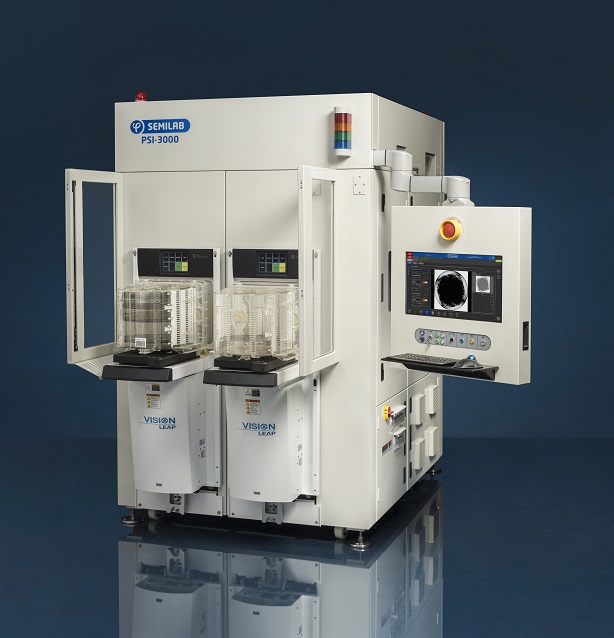 Figure 1. PSI-3000