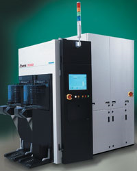
SW-3300
The Semilab AMS SW-3300 uses the exclusive SurfaceWave™ technology to measure the thickness and uniformity of thin film metals and dielectrics. It’s a low cost but powerful product built expressly for copper, low k materials. It is a superior measurement of bottle trench, straight trench, dielectric layer thickness and composition.
Features and System specifications:
- Metrology for mixed 200/300 or 150/200 mm wafers
- Robust, solid-state lasers with lifetime greater than 1 year
- Precise and repeatable pattern measurement
- Lowest ownership cost of any non-contact system on the market
- Easy to use
- Proven track record of reliability
- Semilab AMS quality and durability
- SEMI S2/S8 and CE compliant Fed 209E Class 1 mini-environment (ISO Class 2) 300mm GEM automation standards.
Dual load port configurable as:
- Dual FOUP
- Dual SMIF
- FOUP & SMIF bridge tool
- Open cassette
Semilab AMS SW3300A
The advanced SW 3300A was announced mid-year 2007. It contains the same features as the SW 3300, and adds multiple layer measurements.
Request Info


