


Application
EPI THICKNESS MEASUREMENT
A blanket layer of silicon can be added to a silicon substrate by a CVD process to achieve changes in the properties, like resistivity, type and defect density. This CVD process is called epi (or epitaxial) deposition. The thickness monitoring of the epi layer is part of the production process of making the epi wafers. This monitoring is executed on a sample basis, or only to confirm that the epi reactor is set up properly.
Semilab can offer non-contact optical solution for Epi thickness monitoring, depending on infrared reflection techniques.
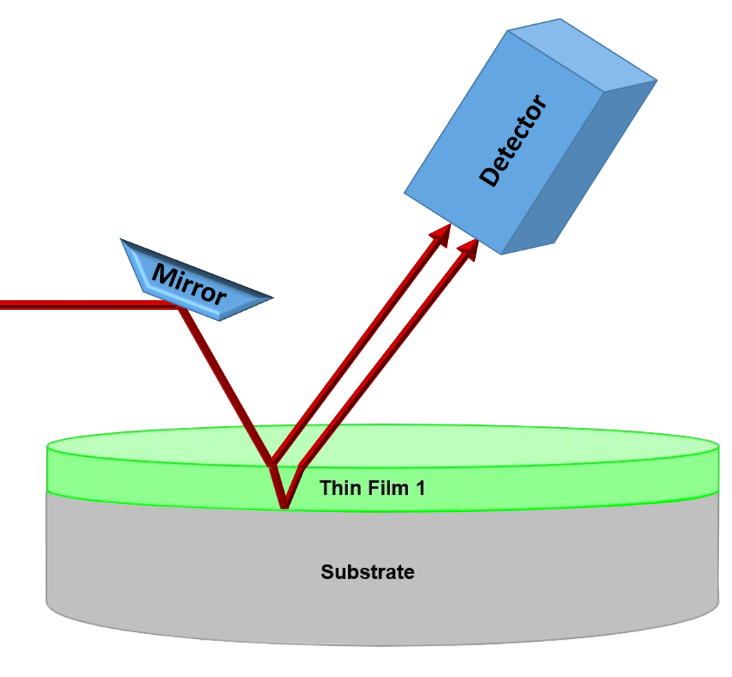 Figure 1. Epi deposition