


Application
OFFLINE PROCESS CONTROL
The best quality control can be achieved by inline process monitoring to check every wafer in the manufacturing process. However, in some cases the short cycle time (usually less than 1 second) does not allow to realize detailed analysis of the wafer, which may include full wafer mapping and techniques requires mechanical contacts.
The measurement tools were designed to include non-destructive techniques and favor non-contact methods where possible.
- Fast measurements
- User friendly operation
- Low cost of ownership
The applications include the followings:
- Incoming wafer characterization
- Measurement of electrical parameters in different manufacturing steps
- Characterization of deposited layer parameters
- Monitoring surface passivation efficiency and homogeneity
Technology
FOUR POINT PROBE SHEET RESISTANCE
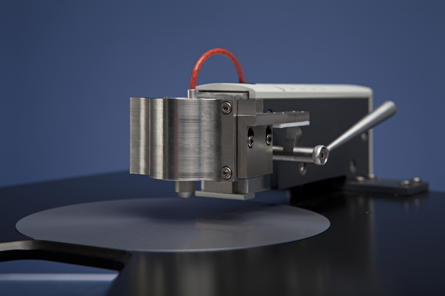
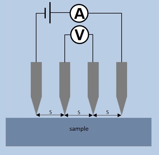
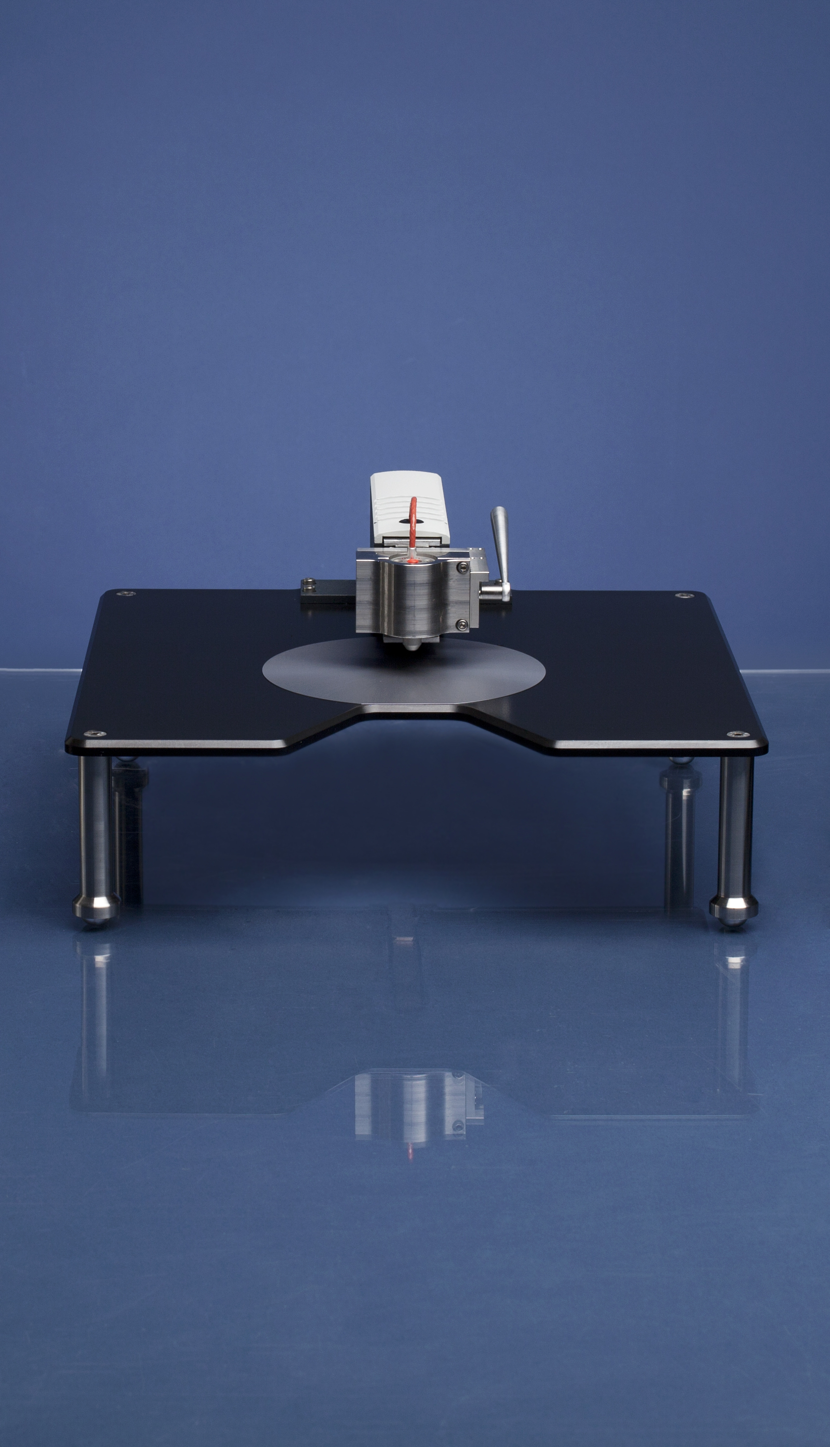
The four point probe (4PP) is a widely used contact technique for monitoring of doping density, resistivity or emitter sheet resistance values. The separation of voltage and current electrodes eliminates the effect of contact resistance from the measurement result. The used voltage is limited so in the high resistivity range the measurable current is getting very small which sets a limitation for the measurement. With our six pin probe (6PP) technique we overcome this problem by using two additional pins to suppress the measurement noise as much as possible.
Metrology overview
The sample is contacted by four pins and a current generator leads a defined current through the sample via the outer pins. The two inner pins are used to measure the voltage between them. From these two parameters, the sample’s sheet resistance can be calculated. The space between the pins is equal (1mm for 4PP and 1.5mm for 6PP). The pin material is produced from tungsten carbide (4pp) and stainless steel (6pp). In case of 4pp the contact force and the curvature of the pins can be chosen as required for a given material. Periodical calibration isn’t necessary for this kind of measurement technique because it’s based upon self-calibration.
FEATURES
- Extended measurement range with 6PP up to 1TΩ/sq
- Wide selection of pin’s curvature and probe force in order to get precise result with minor destruction
Product Line
WT, FPP
The FPP product line uses a simple, easy to use measurement method, well suited to measure semiconductor resistivity and sheet resistance of thin films. It can be used to provide standards for other resistivity measurement methods.
The WT product line is a powerful measurement platform for performing many different semiconductor material characterization measurements. The base system includes all the overhead functions necessary to perform characterization measurements, including power supplies, computer and operating software, XY measurement stage, etc.
The WT-2000 is typically used to make maps, where the wafer is scanned at a programmable raster. Each system is configured to the user’s requirements by adding treatment and measurement capabilities.
WT-1200 series are non-contact bulk lifetime and resistivity measurement tools developed specially for mono-crystalline ingots and slugs.
Products

FPP-1000
FPP-1000 is standalone platform with built-in, conventional four-point probe head. It uses an absolute measurement method without recourse to calibrated standards.
Features and System specifications:
- Sheet resistance range: 0.1 mΩ/sq – 50M Ω/sq
- Max. Touchdowns: ~100.000
- Tip material: Tungsten carbide
- 4 Point Probe head options:
- Spacing: 0.500, 0.635, 1.000, 1.591 mm (default: 1 mm)
- Load force: 10-150g (default: 100g)

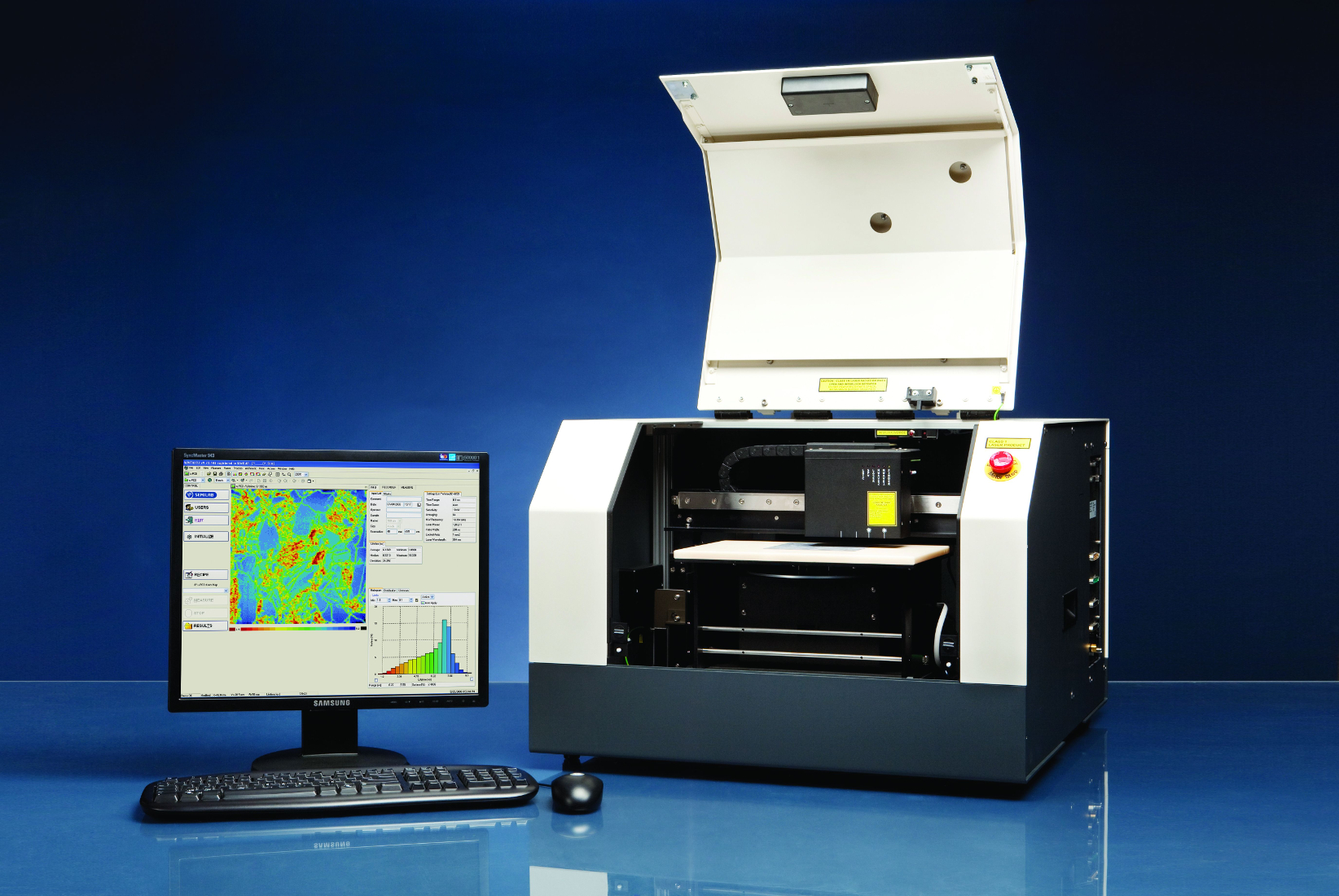
WT-2000 Wafer Tester - Tabletop System
The WT-2000 is a powerful tabletop measurement platform for performing many different semiconductor material characterization measurements. The base system includes all the overhead functions necessary to perform characterization measurements, including power supplies, computer and operating software, X-Y measurement stage and so on. It is typically used to make maps, where the wafer is scanned at a programmable raster. The WT-2000 can also perform measurements at specific, programmable measurement locations.
The WT-2000 is suggested for mid-range fabs and laboratories.
Features and System specifications:
- Wafer size: up to 300 mm with bare or dielectric coated surface
- Wafer handling: manual or Semilab-made indexer
- Loading options:
- 100-200 mm cassette indexer
- 300 mm 13 slot cassette indexer, including open cassettes for 100-300 mm wafers
- 300 mm 25 slot cassette indexer, including FOUP, FOSB, and open cassettes for 100-300 mm wafers
- Samples: np junction (implanted, annealed)
- Automation software with SECS/GEM communication option for non 300 mm standards.
- Factory automation: SECS/GEM for not 300 mm standards
Each system can be configured based on the user’s requirements by adding measurement capabilities and automation capabilities described below.
Measurement capabilities:
- µ-PCD for measuring carrier lifetime
- SPV for measuring diffusion length
- JPV for measuring ion implants
- Eddy current measurement of sheet resistance
Request Info

WT-2000PVN
The WT-2000PVN is a table top measurement system, capable of performing a variety of measurements on PV cells, wafers, and blocks. The base system includes the overhead functions, and you configure the measurement capabilities to match your specific needs, by selecting from the options below.
The WT-2000PVN can measure blocks and ingots, as well as wafers and cells. For measuring wafers and cells, people typically produce maps. When measuring blocks or ingots, people often produce only line scans, to save time, WT-2000PVN can do both.
Most producers of PV cells own a WT-2000PVN. It is extremely useful for:
- Engineering development and characterization
- Batch testing of production
- Comprehensive troubleshooting of production problems
Measurement techniques that can be integrated in WT-2000PVN:
- µ-PCD / carrier lifetime
- Measured parameter: carrier lifetime
- High resolution mapping and discrete point measurements
- SHR / sheet resistance
- Measured parameter: emitter sheet resistance
- Mapping and discrete point measurements
- LBIC / photovoltaic response, quantum efficiency, diffusion length
- High resolution mapping with 1 to 4 lasers
- Measured parameters:
Short circuit current
Direct and scattered reflectance
IQE and EQE
Diffusion length
- Eddy current
- Non-contact resistivity mapping
- Different resistivity range probes
- Bias light to µ-PCD