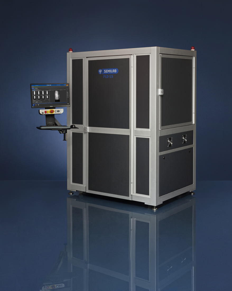
PLB-55 Photoluminescence Silicon Block Imaging System
PLB is fast, non-contact, easy-to-use system to detect defects and impurity concentration in silicon blocks for photovoltaic application.
Features and System specifications:
Ingot Imaging system:
- Photoluminescence lifetime measurement - mapping for all 4 sides
- Max block size: 159×159×500 mm
- Block type: polished or non-polished block
- IR transition based inspection
- Built in integrated μ-PCD lifetime measurement with 1 probe for in-situ calibration - 1 line scan per side and lifetime calibration of the entire PL image.
- Block size determination with built Omron optical sensors
- Built in eddy head for resistivity measurement 1 line scan per side
- Built in P/N tester for conductivity type determination 1 line scan per side.
- Weight measurement (Max. 50 kg, 20 g accuracy)
Additional Measurements:
- Resistivity measurement with eddy head
- Lifetime measurement with μ-PCD head
- Temperature measurement with pyro sensor
- PN conductivity type measurement
- Block weight measurement
- Block size measurement
- Block angle measurement
Software evaluation:
- Calculated lifetime map
- Determination of the cutting line based on lifetime
- Determination of the cutting line based on resistivity
- Defect area percentage
- Colored images
- Export data to Excel
Options:
- High resolution images (transmission, PL)
- Fully automated robot support
- Block marker and printing
- G-code for CNC machines
- MES
- Slug measurement for R&D
- Language options: English, Chinese, Hungarian, for other, please contact us


