Application
OFFLINE PROCESS CONTROL
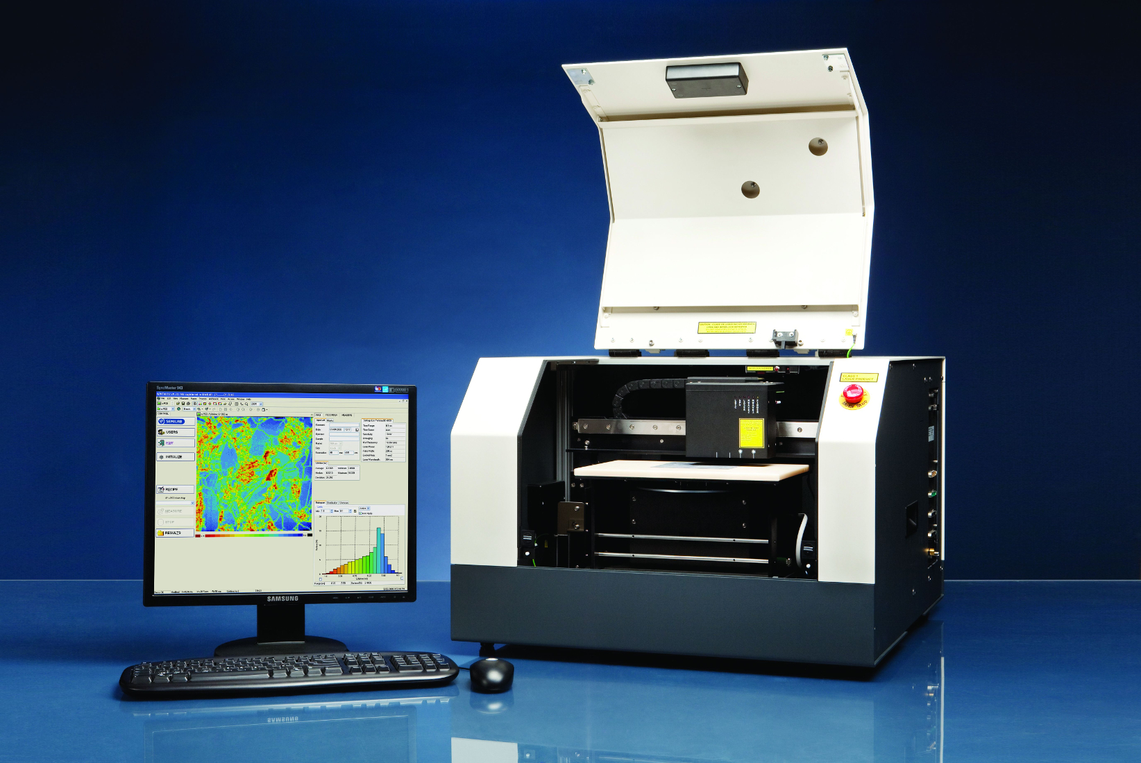
The best quality control can be achieved by inline process monitoring to check every wafer in the manufacturing process. However, in some cases the short cycle time (usually less than 1 second) does not allow to realize detailed analysis of the wafer, which may include full wafer mapping and techniques requires mechanical contacts.
The measurement tools were designed to include non-destructive techniques and favor non-contact methods where possible.
- Fast measurements
- User friendly operation
- Low cost of ownership
The applications include the followings:
- Incoming wafer characterization
- Measurement of electrical parameters in different manufacturing steps
- Characterization of deposited layer parameters
- Monitoring surface passivation efficiency and homogeneity