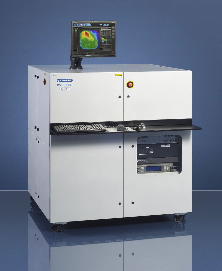
PV-2000A
Features and System specifications:
It is a new integrated platform with the following capabilities:
- SPV Diffusion Length
- Discrete ites and mapping of incoming and processed wafers to final cells.
- UV/Blue SPV ratio for surface passivation (arb. units)
- Monitorable parameters:
- Diffusion length (L)
- Fe contamination (Fe)
- Other Recomb. Centers (NR)
- LID Defect Contamination
- Noncontact C-V profiling
- Time resolved approach with leakage correction
- Monitorable parameters:
- Flatband Voltage (Vfb)
- Oxide Total Charge (Qtot)
- Interface Trapped Charge (Qit)
- Interface Trap Density (Dit)
- Dielectric Capacitance (CD) and thickness (CET),
- Dielectric Leakage and PID testing 3 to 1000 nm planar and textured films
- Accelerated LID testing
- Temperature stages (20-220°C), 2 illumination stations (halogen and flash); robotic handling: activates/deactivates iron and/or boron-oxygen
- LID defects in minutes
- ALID is sequenced with SPV for Fe and LID defect mapping in short time
- Applicable to wafers and solar cells
- QSS-μPCD
- Discrete sites and mapping of incoming and processed wafers
- PCD laser wavelength: 904 nm
- Monitorable parameters:
- Decay lifetime (τ eff.d)
- Steady-state lifetime (τ eff.ss)
- Injection level (Δn)
- Effective surface recombination (Seff)
- QSS light intensity: 0.005 to 30 Suns
- Emitter Saturation Current (J0)
- Implied Voc
- Light Beam Induced Current (LBIC)
- Mapping of solar cells 1 to 4 lasers
- Measurement parameters: Current; Diffusion Length; Reflectance; Internal Quantum Efficiency (IQE)
- Reflectance measurement and IQE mapping
Other testing capabilities:
- SPV Surface Lifetime
- SPV Mapping of Rshunt and Voc
- Noncontact Suns-Voc
- Wafer Thickness Measurement


