


Application
LABORATORY APPLICATIONS
Troubleshooting manufacturing process needs more comprehensive analysis of the wafers in different process steps. Often these tests are out of scope of in-line and offline process control tools. For this purpose Semilab can offer state-of-the art laboratory tools with multiple capabilities.
These advanced metrology tools can be effectively used in the research and development field to introduce new methods and techniques for high efficiency solar cell production.
Semilab is open for cooperation with customers to improve the tool performance and introduce new applications to cover future metrology needs.
The measurement tools were designed to achieve good tool performance, user-friendly operation and low cost of ownership.
The applications include the following:
- Wafer contamination characterization
- Analytical contamination detection in wafers
- Measurement of electrical parameters in different manufacturing stages
- Optical characterization of deposited layer parameters
- Electrical characterization of deposited dielectric layer parameters
- Measuring surface passivation efficiency and homogeneity
- Testing accelerated light-induced degradation (LID) and potential-induced degradation (PID) of solar cells
Technology
NON-CONTACT C-V PROFILING
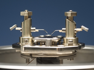
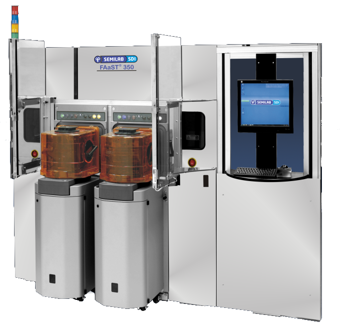
Semilab SDI FAaST systems represent state-of-the-art non-contact electrical metrology used in manufacturing control and development of semiconductor devices and materials. Employing non-contact surface potential probing techniques combined with illumination and/or non-invasive surface charging, these powerful techniques measure a broad range of parameters characterizing semiconductor wafers, dielectrics and interfaces with astounding precision, while saving the cost and time involved in fabricating dedicated test devices.
The major application of the Non-Contact C-V profiling metrology is monitoring of dielectrics during IC manufacturing. The most important feature, differentiating it from conventional electrical measurements, is its preparation free non-contact nature, which eliminates preparation of MOS capacitors, thereby reducing metrology cost and facilitating fast data feedback in both Manufacturing and R&D environments.
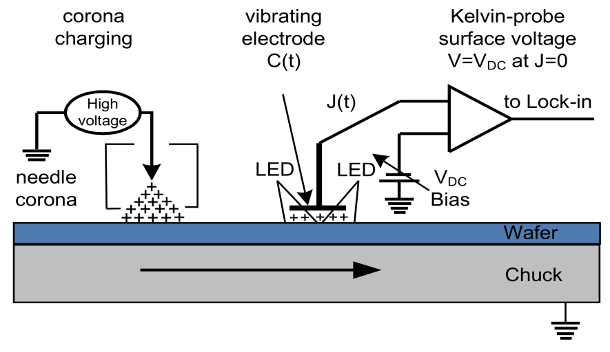
The non-contact corona-Kelvin metrology uses corona discharge in air to place an electric charge on a semiconductor wafer. The wafer response is monitored with a vibrating capacitor probe, typically a Kelvin-probe, which measures the surface voltage (Vcpd). Surface voltage monitoring in both the dark and under strong illumination enables separation of two important voltage components:
- Dielectric voltage (VD)
- Semiconductor surface potential (Vsb)
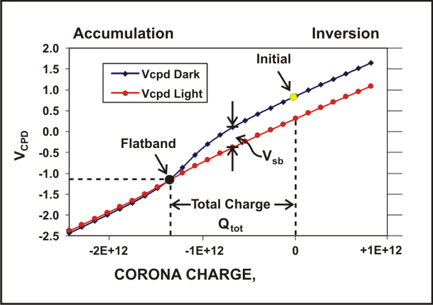
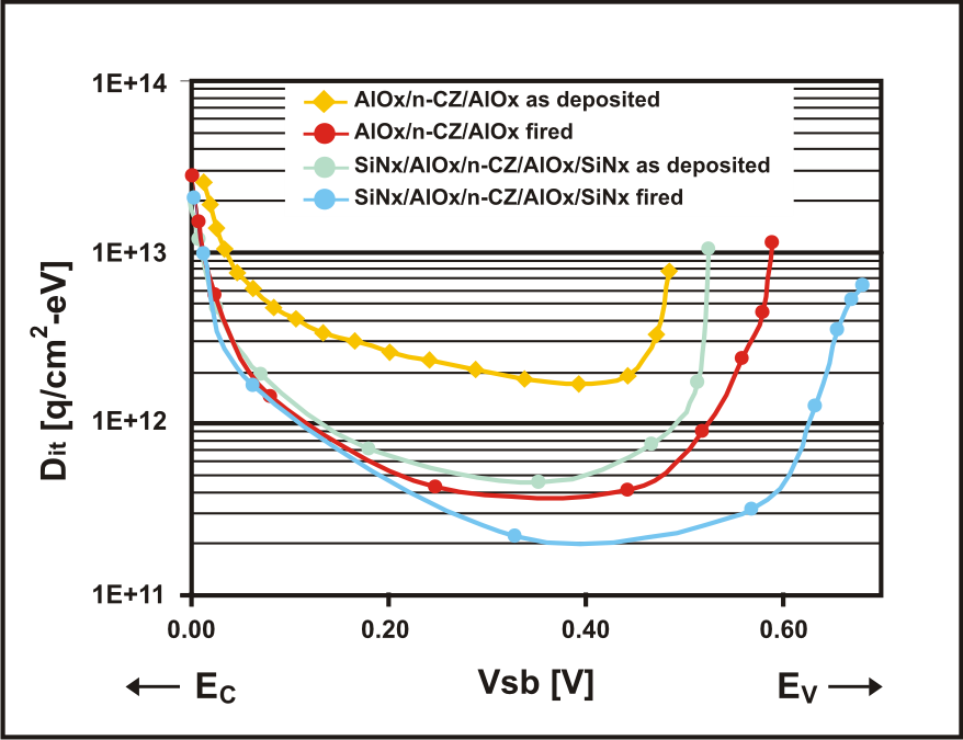
Analysis of the acquired charge-voltage data provides electrical parameters such as Dit, Vfb, Qtot (dielectric charge), CD, EOT, and Dielectric Leakage.
Example Vcpd vs Qcorona data for dielectric on p-type Si
Example Dit spectra for various dielectrics on Si
The major application of this metrology is monitoring of dielectrics during IC manufacturing. The most important feature, differentiating it from conventional electrical measurements, is its preparation free non-contact nature, which eliminates preparation of MOS capacitors, thereby reducing metrology cost and facilitating fast data feedback in both Manufacturing and R&D environments.
FEATURES
- Non-contact electrical C-V and I-V metrology providing characterization of dielectrics and interfaces with unparalleled accuracy and precision for the IC manufacturing and R&D environment
- Available in Macro configuration for measurements on Monitor wafers
- Unique Micro configuration option using Kelvin Force Microscopy (KPFM) measures C-V and I-V characteristics in scribe-line test sites and in active device areas on Production wafers
- Demonstrated inter-fab Tool to Tool Matching
- Time-resolved voltage measurements enable dielectric leakage determination and corresponding leakage-corrected true C-V curve measurement for sub-nanometer dielectrics
- Proprietary C-V simulator for dielectric capacitance extraction that works in the presence of very large interface trap density
- Proven applications for advanced ultra-thin dielectrics, high k dielectrics, and inter-layer dielectrics
- Excellent correlation to End-Of-Line device data
Product Line
PV
FAaST metrology includes best in the world Semilab SDI unique capabilities:
- The Digital Surface PhotoVoltage, DSPV, measurement of minority carrier diffusion length with unmatched sensitivity for Fe detection in Si wafers.
- Corona-Kelvin characterization of dielectrics and interfaces with capability for pattern wafer measurement and micro-scale scribe-line (SL) measurement using micro-corona and Kelvin Force Probe Microscopy (KPFM).
- Wafer mapping is available for all measured parameters and especially high-throughput mapping of non-visual defects including electrical charge defects caused by plasma etching, ion implantation, or mobile ion contamination.
Semilab SDI FAaST system’s offer:
- Flexible configurations that can be customized to suit individual customers’ needs.
- Platforms range from a fully automated dual 300mm loadport system configured with all measurement options and capable to meet the 300mm Semi requirements of modern IC Fabs to manual load systems configured with a single measurement technology that can measure samples as small as ~20mm x 20mm making them well suited for the University or Laboratory environment.
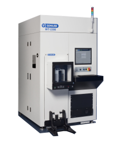
The WT product line is a powerful measurement platform for performing many different semiconductor material characterization measurements. The base system includes all the overhead functions necessary to perform characterization measurements, including power supplies, computer and operating software, XY measurement stage, etc. The WT-2000 is typically used to make maps, where the wafer is scanned at a programmable raster. Each system is configured to the user’s requirements by adding treatment and measurement capabilities.
Products
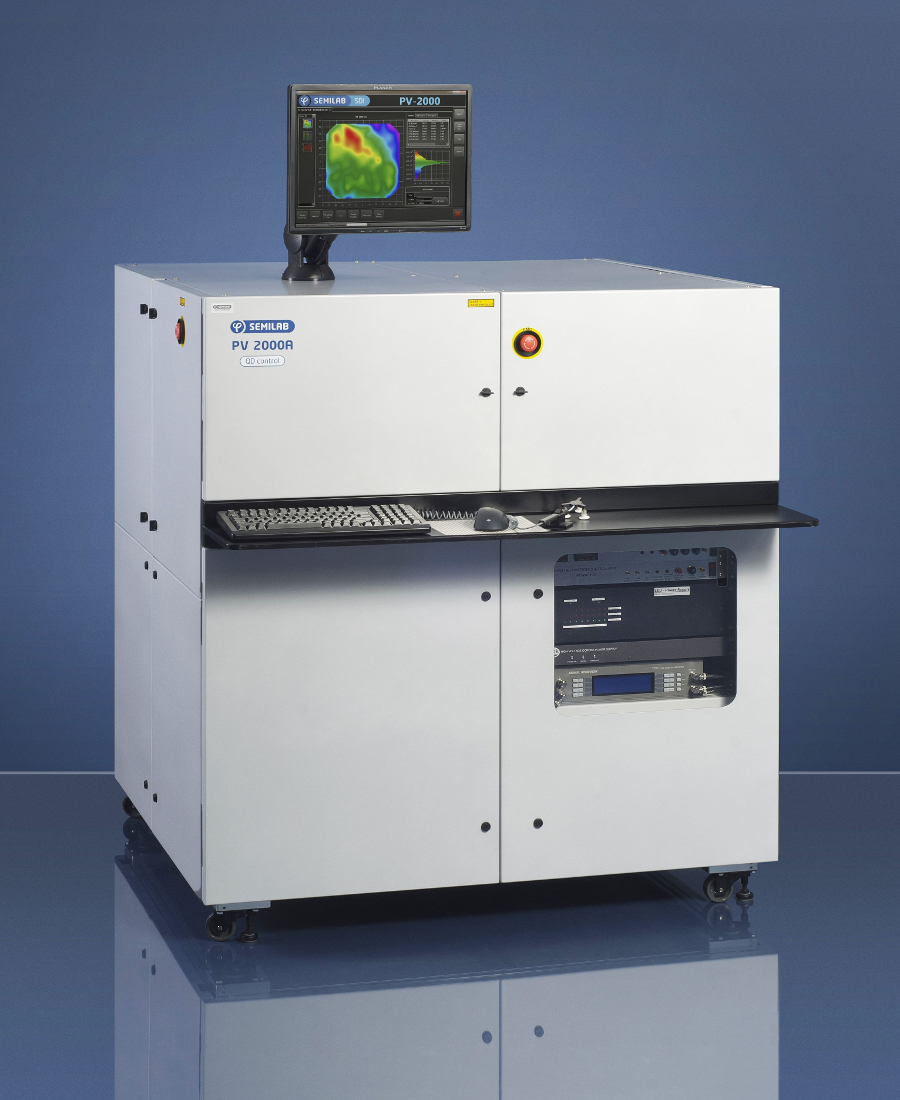
PV-2000A
Features and System specifications:
It is a new integrated platform with the following capabilities:
- SPV Diffusion Length
- Discrete ites and mapping of incoming and processed wafers to final cells.
- UV/Blue SPV ratio for surface passivation (arb. units)
- Monitorable parameters:
- Diffusion length (L)
- Fe contamination (Fe)
- Other Recomb. Centers (NR)
- LID Defect Contamination
- Noncontact C-V profiling
- Time resolved approach with leakage correction
- Monitorable parameters:
- Flatband Voltage (Vfb)
- Oxide Total Charge (Qtot)
- Interface Trapped Charge (Qit)
- Interface Trap Density (Dit)
- Dielectric Capacitance (CD) and thickness (CET),
- Dielectric Leakage and PID testing 3 to 1000 nm planar and textured films
- Accelerated LID testing
- Temperature stages (20-220°C), 2 illumination stations (halogen and flash); robotic handling: activates/deactivates iron and/or boron-oxygen
- LID defects in minutes
- ALID is sequenced with SPV for Fe and LID defect mapping in short time
- Applicable to wafers and solar cells
- QSS-μPCD
- Discrete sites and mapping of incoming and processed wafers
- PCD laser wavelength: 904 nm
- Monitorable parameters:
- Decay lifetime (τ eff.d)
- Steady-state lifetime (τ eff.ss)
- Injection level (Δn)
- Effective surface recombination (Seff)
- QSS light intensity: 0.005 to 30 Suns
- Emitter Saturation Current (J0)
- Implied Voc
- Light Beam Induced Current (LBIC)
- Mapping of solar cells 1 to 4 lasers
- Measurement parameters: Current; Diffusion Length; Reflectance; Internal Quantum Efficiency (IQE)
- Reflectance measurement and IQE mapping
Other testing capabilities:
- SPV Surface Lifetime
- SPV Mapping of Rshunt and Voc
- Noncontact Suns-Voc
- Wafer Thickness Measurement