


Application
DEFECT INSPECTION
“Bulk Micro Defects” (BMD) is a term commonly used to refer to oxygen precipitates in silicon. In fact, many imperfections in the silicon lattice create defects, and BMDs could be any imperfections including oxygen precipitates, voids, inclusions and so on.
BMDs go by many names, referring to the problems they cause, how they were created, or their physical characteristics. Examples include COPs (Crystal Originated Particles) and Grown-In Defects.
Dislocations can be formed during crystal growth, but also at thermal processing of wafers, during CMOS device manufacturing, like epitaxial layer growth and implant anneal steps.
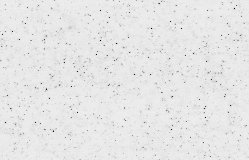
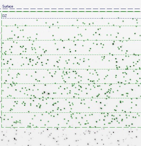 Figure 1. Bulk Micro Defects
Imperfections in the lattice of a semiconductor and impurities create energy states in the bandgap, decrease carrier lifetime, and increase junction leakage. They also act as gettering sites, at which impurities tend to concentrate. The profile of the BMDs is often controlled as shown in Figure 1. by a complex series of high temperature processes to create a “denuded zone”. By this, the surface layer silicon, where the MOS transistor action takes place is free of oxygen precipitates, and the oxygen precipitates in the underlying silicon act as a gettering site to keep impurities away from the MOS transistors.
IR light penetrates most semiconductor materials, and since BMDs alter the local optical properties of a semiconductor, BMDs can be detected by illuminating a sample with IR light and looking at it with a camera that is sensitive to IR.
Technology
LOW-ANGLE LIGHT SCATTERING TOMOGRAPHY
Light Scattering Tomograph enhanced with Low-angle illumination (LSL) technology is a Bulk Micro Defect (BMD) inspection system of SEMILAB, which is suited especially for patterned wafers.
Throughout numerous processes of integrated device creation, various thermal impacts affect a wafer. The number and size of BMDs change constantly based on the sample’s thermal history. Thermal treatment can be applied using a furnace, which is equivalent to the effects of real production. These heat-treated samples are then measured by the LST system to determine the size and density distributions of BMDs. However, tier one integrated device manufacturers want to measure real production patterned wafers in failure analysis. The LST cannot measure patterned samples, but the LSL can.
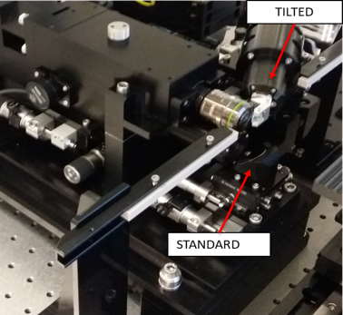
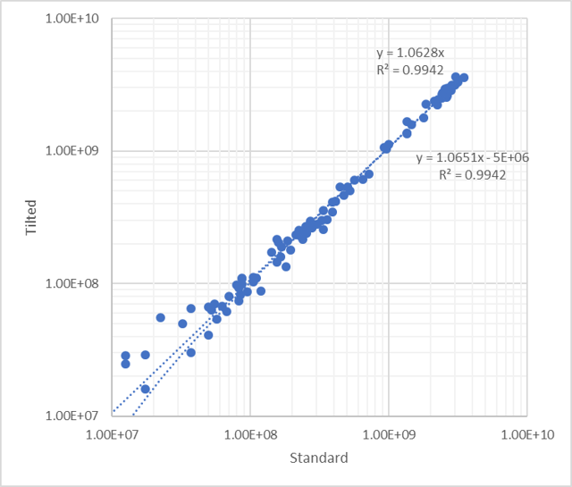
Its special dual illumination unit allows BMD detection in Standard mode (for bare wafers) and in Tilted mode (for patterned wafers), while the two measurement modes show perfect correlation.
LSL is based on the laser scattering tomography principle.
After the autofocus and the laser power setting procedures, the focused infrared laser beam illuminates the scatterers (like precipitates, dislocations and stacking faults) in the bulk, close to the cleaved surface of the semiconductor wafer. In normal mode, the illumination is applied via the top surface of the sample, while in low-angle mode via the cleaved surface. The scattered light is collected with a high NA objective and the image is detected with near infrared sensitive CCD camera. The image is taken by X scanning of the wafer placed on the motorized sample stage.
The software calculates the defect density for each size and creates a histogram. In automatic mode, the analysis software can run parallel to the image acquisition, processes LST images and creates Excel compatible tabulated text output of defect statistics of important parameters, such as density and size. (see Figure 2. and Figure 3.)
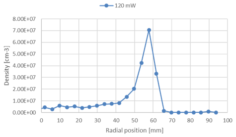 Figure 2. Densitiy radial distribution
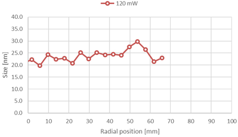 Figure 3. Size radial distribution
Semilab publication
Szarvas et al: Bulk micro-defect detection with low-angle illumination, Review of Scientific Instruments 92, 043701 (2021); https://doi.org/10.1063/5.0027147
FEATURES
- Patterned wafer measurement in low-angle mode
- Combo mode for validation of low-angle illumination results
- Parallel data acquisition and evaluation (no extra time needed)
- Excellent reproducibility allows the measurement of the size of the same individual defect before and after thermal treatment
- Effective automated measurement and counting of BMD data
- Various reporting possibilities on defect statistics and DZ
- Outstanding stability and Tool-to-Tool matching
- Engineer-independent adjustment procedures
Product Line
LSL
Light Scattering tomograph enhanced with Low-angle illumination (LSL) is a powerful equipment for monitoring Bulk Micro Defect (BMD) profile in bare and patterned silicon samples. BMDs scatter the incident light, which is recorded by a CCD camera near to the cleaved edge of the sample.
LSL captures 2000 × 400 μm darkfield images of the scattered intensity from the wafer. BMDs form peaks on this intensity map, and are detected by automatic defect-finding algorithm. The evaluation software then calculates the number of defects, the density and the size depth distribution and size histogram.
Normal mode
In normal mode, the focused infra-red laser beam illuminates the scatterers (like precipitates, dislocations and stacking faults) via the top surface close to the cleaved surface of the semiconductor wafer. This illumination unit is the same as it is applied in the LST system. Results obtained in this mode is fully equivalent to LST results.

Low-angle mode
In low-angle mode, the illumination is applied via the cleaved surface under a low-angle, the illumination line is generated by a cylindrical lens. It enables the machine to measure patterned wafers, which cannot be measured by standard LST system.
Combo mode
In combo mode, the image is taken twice: first in normal mode, then in low-angle mode. The comparison between the reported densities then can be carried out easily. The correlation between two measurement modes can be determined for bare wafers. It validates the low-angle illumination mode and the results obtained for patterned wafers are reliable.
Products

LSL-2500
LSL-2500 is a unique metrology system on the semiconductor market. Its special dual illumination unit allows BMD detection in Standard mode (for bare wafers) and in Tilted mode (for patterned wafers), while the two measurement modes show perfect correlation.
Since LSL is a sister development of the industry standard LST-2500HD system, LSL is dedicated to being the reference technique of BMD control on bare and patterned wafers as well.
| LSL-2500 | |
|---|---|
| Area of application | IC makers / Wafer fabs / R&D |
| Wafer handling | Automated loading |
| Sample positioning |
Advanced autofocus mechanism |
| Scanning range |
Whole wafer diameter scan** |
| Evaluation |
Automatic evaluation parallel with measurements |
| Denuded zone |
DZ determination from one image (only in normal mode) |
| Reporting functions (single point) |
Density, size depth profile, size histogram |
| Reporting functions (radial scan) |
Average density, average size, DZ radial distribution |
**excluding bad edge area
Request Info