


Application
DEFECT INSPECTION
“Bulk Micro Defects” (BMD) is a term commonly used to refer to oxygen precipitates in silicon. In fact, many imperfections in the silicon lattice create defects, and BMDs could be any imperfections including oxygen precipitates, voids, inclusions and so on.
BMDs go by many names, referring to the problems they cause, how they were created, or their physical characteristics. Examples include COPs (Crystal Originated Particles) and Grown-In Defects.
Dislocations can be formed during crystal growth, but also at thermal processing of wafers, during CMOS device manufacturing, like epitaxial layer growth and implant anneal steps.
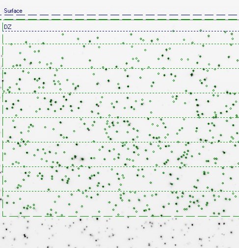 Figure 1. Bulk Micro Defects
Imperfections in the lattice of a semiconductor and impurities create energy states in the bandgap, decrease carrier lifetime, and increase junction leakage. They also act as gettering sites, at which impurities tend to concentrate. The profile of the BMDs is often controlled as shown in Figure 1. by a complex series of high temperature processes to create a “denuded zone”. By this, the surface layer silicon, where the MOS transistor action takes place is free of oxygen precipitates, and the oxygen precipitates in the underlying silicon act as a gettering site to keep impurities away from the MOS transistors.
IR light penetrates most semiconductor materials, and since BMDs alter the local optical properties of a semiconductor, BMDs can be detected by illuminating a sample with IR light and looking at it with a camera that is sensitive to IR.
Technology
LIGHT SCATTERING TOMOGRAPHY
The light scattering tomography technique is a powerful way to detect defects in bulk monocrystalline materials, in the few tens of nanometers range. As the inspected material is mainly silicon, using proper infrared illumination light can be focused into the sample and Rayleigh-scattered light can be collected. The darkfield arrangement ensures that the low level scattered light suffers minimal disturbance from the defect due to the illumination, applying low noise and highly sensitive infrared detection. Our Light Scattering Tomograph (LST) tool can be applied for analyzing as-grown monosilicon materials, and also for heat-treated samples, samples with epitaxial layer and oxide layer. The tool supports fully automated loading and unloading of half cleaved samples from special designed cassettes, automatic data evaluation and various result output. Individual measurement sites can be analyzed manually in detail, or in production use the data can be analyzed automatically based on pre-defined image processing recipes.
The LST is an excellent tool to identify crystal-growth defects like voids, interstitial silicon and oxygen precipitates. Voids or vacancies are created when v/G is large. As they agglomerate, they change the optical properties of the material, and they can be detected by light scattering. Oxygen precipitates are formed due to heat treatment. They also change optical properties of the material.
LST is based on laser scattering tomography principle. After the autofocus procedure and the laser power setting the focused infrared laser beam illuminates the scatterers (like precipitates, dislocations and stacking faults) in the bulk, close to the cleaved surface of the semiconductor wafer. The perpendicular scattered light is collected with high NA objective and the image is detected with near infrared sensitive CCD camera. The image is taken by X scanning of the wafer placed on the motorized sample stage.
The software calculates the defect density for each size and creates a histogram. In automatic mode, the analysis software can run parallel to the image acquisition, processes LST images and creates Excel compatible tabulated text output of defect statistics of important parameters, such as density and size (see Figure 2. and Figure 3.).
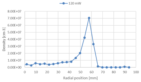 Figure 2. Densitiy radial distribution
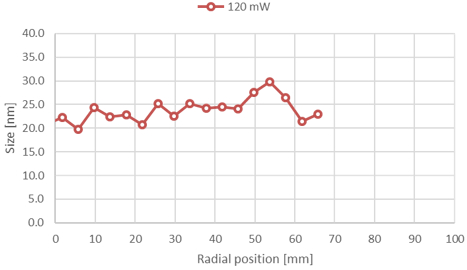 Figure 3. Size radial distribution
References:
1. Tamás Szarvas et al., Application of light scattering tomography for Si(111) samples, Review of Scientific Instruments 92, 053701 (2021)
2. Ferenc Korsós et al., Efficiency limiting crystal defects in monocrystalline silicon and their characterization in production, Solar Energy Materials and Solar Cells 186, 217–226 (2018)
3. Vanessa Monier et al., Light scattering from dislocations in silicon, Journal of Applied Physics 108, 093525 (2010)
FEATURES
- Effective automated measurement and counting of BMD data
- High sensitivity
- High dynamic range (≥ 3) to cover the widest size range available with one laser power settings
- Improved resolution for high density wafers
- Excellent reproducibility allows the measurement of the size of the same individual defect before and after thermal treatment
- Scanning of the illumination plane can provide tomography function
- Various reporting possibilities on defect statistics and DZ
- Outstanding stability
- Perfect Tool-to-Tool matching
- Engineer-independent adjustment procedures
- Beam characterization: improved beam diameter measurement, beam shape and tilt measurement
Product Line
LST-HD
The Light Scattering Tomograph (LST) is a powerful tool for monitoring Bulk Micro Defect (BMD) profile of silicon samples. The BMD scatters the incident light, which is recorded by a CCD camera near to the cleaved edge of the sample.
LST captures 2000 × 400 μm darkfield images of the scattered intensity from the wafer. BMDs form peaks on this intensity map, and are detected by automatic defect-finding algorithm. The evaluation software then calculates the number of defects, the density and the size depth distribution and size histogram.
The Denuded Zone (DZ), which is the defect-free zone below the wafer surface is also determined and reported by the software.
Due to our continuous improvement program, LST has been acquired superior performance in all important features that a light scanning tomograph can have.
All these achievements are encrypted in the acronym HD, which represents the following features:
HD – High Dynamic range
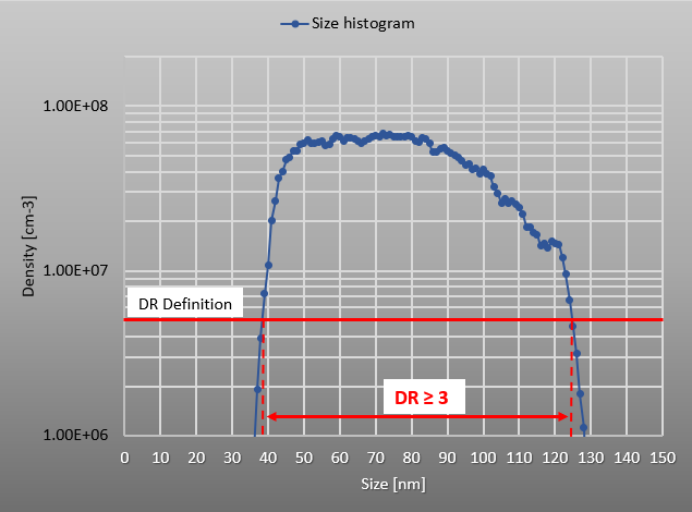
Samples contain BMDs in various sizes, from a few to hundreds of nanometers. BMDs are detected by a selected laser power. These are above the search threshold (minimum size) and below the saturation limit (maximum size). It is better to measure wider size range at once. The Dynamic Range (DR) is defined for the LST according to the ratio of the maximum and minimum size values. DR for LST-2500HD is proven to be ≥ 3 (see Figure). It indicates that the standard size range can be covered only by two recipes.
HD – High Detectability
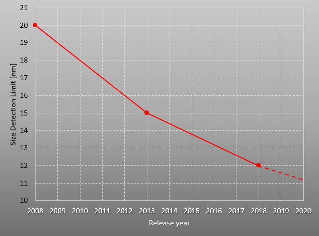
Like in other metrology techniques, the detection of the even smaller BMDs is pursued with the LST by achieving even higher sensitivities. The more than 10 years experience between wafer makers and Semilab (hundreds of demo measurements and tens of onsite tools) results in continuous improvement in sensitivity (see Figure). BMDs can be detected with the High Sensitivity mode of the LST-2500HD (see Figure). It enables the tool to measure not only heat-treated samples but those without heat treatment or as-grown samples.
HD – High Detection speed
The measurement speed has been accelerated providing excellent throughput even though micron accuracy positioning is necessary in height direction and sub-micron accuracy in the focal direction.
Products

LST-2500HD Light Scattering Tomograph High Dynamic-range System
| LST-2500HD | ||
|---|---|---|
| Area of application | Wafer fabs / R&D | |
| Wafer handling | Automated loading | |
| Sample positioning |
Advanced autofocus mechanism |
|
| Scanning range |
Whole wafer diameter scan** |
|
| Evaluation |
Automatic evaluation parallel with measurements |
|
| Denuded zone |
DZ determination from one image |
|
| Reporting functions (single point) |
Density, size depth profile, size histogram |
|
| Reporting functions (radial scan) |
Average density, average size, DZ radial distribution |
|
**excluding bad edge area
Request Info