


Application
COMPOUND MATERIAL CHARACTERIZATION
Compound materials enable the production of advanced, easy-to-use power devices, ultra-high frequency radio devices and more. These emerging products become more and more prevalent in electric or hybrid cars for example, or in power management and distribution devices related to renewable energy sources. For reliable production, composition and defects, dopant concentration, electrical and optical qualities must be regularly monitored. Semilab offers several products for this purpose. Most products are non-contact and non-destructive, and in many cases, they reveal properties directly related to device characteristics or performance.
Technology
NON-CONTACT SHEET RESISTANCE BY EDDY CURRENT
Device makers have a critical need to measure sheet resistance. Knowing it as a function of position (mapping) allows for optimization of epi reactors to maximize yield.
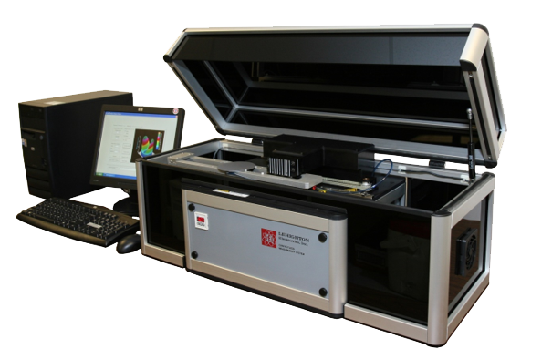
The Semilab LEI-1510 family allows for non-destructive measurement of sheet resistance. These instruments are optimized for compound semiconductor applications with ranges of operation that dovetail nicely with customer applications. The LEI technology became the process of record in the RF device area with many people asking to see the “LEI” map.
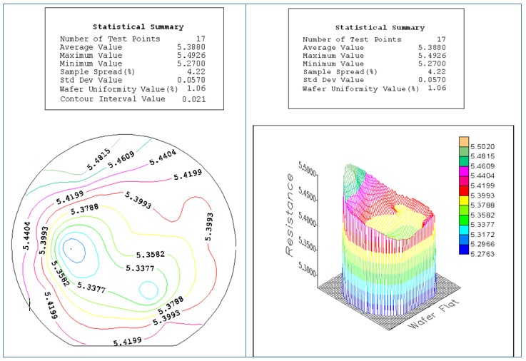 Figure 1. The “Semilab LEI” Maps - the process of record for sheet resitance
The 1510 Non-destructive Sheet Resistance Measurement System uses eddy current to measure sheet resistance.
Resistivity measurement
Theory of resistivity measurement is based on alternating current in a coil (or pair of coils) inducing alternating Eddy current in a conducting material. The Eddy current measurement is actually the measurement of the electrical loss in the material.
The measured signal depends on:
- Resistivity and thickness, in case of samples with finite thickness as wafers
- Sheet resistance, in case of thin layers
- Distance between the coil(s) and sample
The Eddy current is higher in good conducting material compared to less conductive ones.
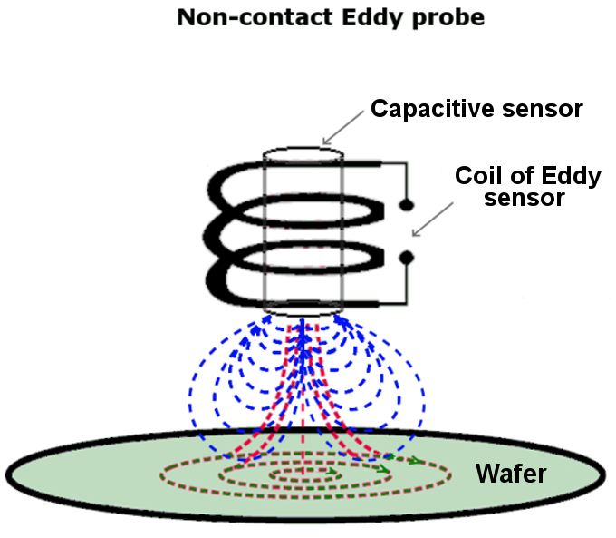
Figure 2. Diagram of Eddy current - upper coil shown only
FEATURES
- Non-destructive
- Non-contact
- No wearing parts unlike 4PP
- Industry standard for RF devices
Product Line
LEI
- Eddy current allows for non-contact sheet resistance
- Ideal for RF device characterization
- Excellent for LED optimization
- Good for metal films on compound characterization
Products

LEI-1510EB, LEI-1510EC
The LEI-1510EC is ideal for both R&D and volume production metrology.
The 1510 as a stand-alone unit is manually loaded and automatically maps. It can accommodate 50-200 mm wafers.
Three ranges of measurement accommodate 0.035 to 3200 Ohm/sq as needed by the application. The EC model is slightly faster than the EB model for those applications where throughput is critical.
Request Info
LEI-1510EC-RP, LEI-1510EC-RS
The LEI-1510 family allows for the best support of high volume manufacturing when paired with a robotic cabinet.
The RP is robotically loaded and accommodates either 50-150 mm or 76-200 mm wafers (option chosen at system build). This system picks and places from a single cassette stand.
The RS expands capability for sorting wafers with a second stand that allows for binning of product into two categories.
Request Info