


Application
INLINE PROCESS CONTROL
Besides Semilab’s own automated wafer sorter platform, Semilab manufactures separate measurement units for integration into automated PV production lines. Semilab has been working together with all the relevant automation companies to integrate the measurement units.
The equipments cover a diverse range of metrology needs for comprehensive process and quality control in Si PV industry:
- Incoming wafer inspection and process control during cell manufacturing
- Measurement in as-cut wafer, textured, after diffusion, after passivation, after ARC deposition, after contact formation states
- Measurements of geometrical, electrical and optical properties
- Solutions for mono and multicrystalline silicon materials, Al-BSF, PERC, IBC and heterojunction cell concepts
All measurement units are designed considering the following directives:
- Compatibility to state-of-the-art production lines
- Supporting all the industry standard communication protocols
- Flexible integration
- Supporting both „on-the-fly” and „stop-and-go” data acquisition modes
- Compact design
- Simple integration and support
- Simple maintenance, rare calibration periods
- Application of noise reduction solutions
- Simple and configurable customization of communication protocols
Technology
THICKNESS AND RESISTIVITY MEASUREMENT
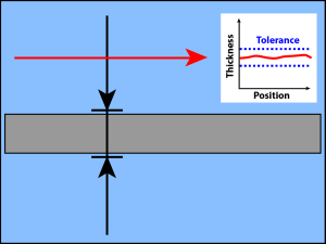
Thickness is a primary control parameter of silicon PV wafers. By filtering out wafers with non-standard thickness and shape, waste from wafer/cell breaking can be reduced.
Thickness of PV wafers is measured for two reasons:
- To insure specification. From the thickness measured in different points of the wafer, the following parameters can be calculated:
- Average thickness
- Total Thickness variation (TTV)
- Thickness Deviation
- To obtain resistivity value by using the Eddy current technique based on thickness information to report the bulk resistivity of the sample.
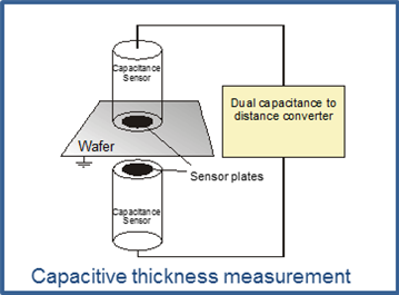
Thickness
WMT/WML uses capacitive probes to measure the distance from wafer surfaces. This way the result is independent on surface quality (reflection).
The capacitance depends on the distance between the probe and the sample:
C = Ɛ . (A/d)
where d is the probe-sample distance. From the measured capacitance the distance can be calculated, and the distances from both sides of the sample makes the thickness determination possible.
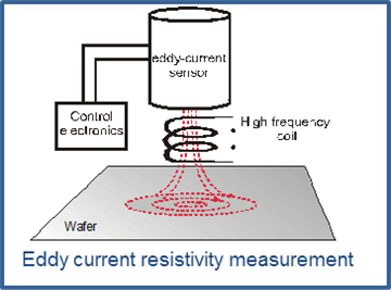
Resistivity
Resistivity measurement is based on non-contact Eddy current method
An AC current flows in a coil in close proximity to a conducting material. The magnetic field of the coil induces circulating (Eddy) currents in the sample. The Eddy current measurement is actually the measurement of the electrical loss in the material, which depends on the resistivity. The signal in the sensor is calibrated to samples certified with 4PP.
The tool measures line scans parallel to the belt direction:
- 6 saw mark line scans (3 on the top, 3 on the bottom)
- 3 thickness line scans
- 1 resistivity line scan
Position of the line scans: 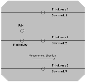
FEATURES
- Non-contact, non-destructive measurement for inline PV applications
- Every single wafer can be measured in production
- No wearing parts unlike 4PP
- Grain size independent resistivity measurement
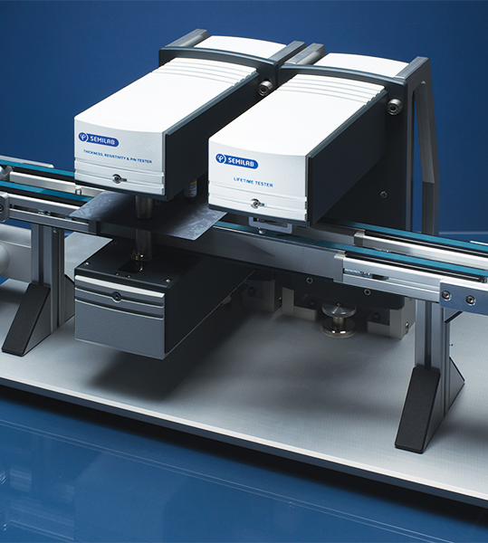
Product Line
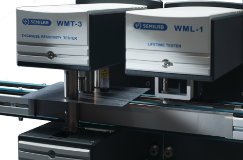
WMT, WLT
WMT/WLT inline tools allow non-contact, preparation free, high-speed thickness and bulk resistivity measurement of crystalline wafers. Robust design and easy integration makes it an obvious choice for wafer sorter applications to sort out of spec wafers. Special design of capacitive probes makes good accuracy even on non-grounded wafers such as in the case of belt transport. Unique design of resistivity sensor makes it independent of grain size variation.
Operating modes and configuration:
- WLT is operating in Stop & Go mode with 1 to 5 thickness sensor pairs and one resistivity sensor
- WMT can measure 1 to 3 line scans in on-the-fly mode with sensor pairs and one line resistivity
Products

TTR-300
The Solar Cell Wafer Topology Measurement system is a complete system for thickness, resistivity and two-sided saw mark measurements.
Features and System specifications:
- Thickness measurement - 6 lines of thickness detection
- Resistivity measurement - 1 line of resistivity measurement along the center line of the wafer with a non-contact Eddy current type sensor.
- P/N determination - conductivity type (P or N) is measured in one point in the middle of the wafer with a non-contact SPV sensor.
- Saw mark - 6 lines of saw mark detection
- The data are transferred to the Data Collector PC

WMT, WLT
Fast non-contact thickness, TTV and resistivity characterization.
Thickness and resistivity are primary quality control parameters for silicon wafers in PV applications.
The WLT models, WLT-1, -3 & -5 In-Line Thickness and Resistivity Testers allow measurement of thickness at 1 to 5 points and resistivity at 1 point with the high throughput that meets the requirements of in-line quality control in fully automated wafer production lines.
The WMT models, WMT-1 & -3, Thickness and Resistivity Testers allow measurement of wafers "on the fly", i.e., conveyor belt does not stop during measurement. Therefore, they have the high throughput that meets the requirements of in-line quality control in fully automated wafer production lines.
Features and System specifications:
- Meas. technique: capacitive thickness and eddy current resistivity
- Sample size: 125 to 156 mm (210 mm option)
- Distance between top and bottom sensors: 2 mm (4mm option for WLT)
- Sample support: on belt
- Calibration: by wafers verified with mechanical gauge and four point probe
Options:
- Measurement module (incl. 1-5 sheet resistance measurement heads)
- Industrial PC (Windows operation system) and peripherals
- P/N conductivity type tester
- Temperature sensor
- Warp & Bow calculation
- Wafer presence sensor (WMT only)
Wide variety of available interfaces to automation and MES:
- 24V optically isolated I/O, Ethernet interface
- Profibus
- OPC DA
- TCP/IP protocol, content can be XML or ASCII
- SQL database
- SECS/GEM