


Application
SI INGOT/ BLOCK TESTING
The quality of the silicon crystal determines the maximum achievable conversion efficiency of the final photovoltaic device. Thus, the quality control of the as-grown Si crystals is crucial to stabilize the manufacturing of modern Si solar cells. Semilab offers various solutions to control all the important material parameters in both multi- and monocrystalline silicon ingots.
Resistivity of the mono and multicrystalline ingots is tested by using eddy current sensor, integrated into various system platforms.
Metallic contamination and extended crystal defects are detected by using different versions of PhotoConductance Decay and Photoluminescence methods.
Finally, our Infrared Imaging system localizes the larger precipitations in the crystal in order to prevent the failures in the wire sawing process.
Technology
E-PCD CARRIER LIFETIME FOR MONO-SI
As the photovoltaic industry moves towards to produce more and more efficient solar cells, the industry requires good quality silicon wafers with high lifetime in larger volume. To the increase the yield of the crystal growing process, new crystal growing techniques were developed, such as CCz. Finding the optimal ingot pulling speed is essential to avoid the formation of precipitations, and to keep the point defect density below the tolerance limit. Since there are many possible failures in the growing procedure, the fast control of the ingot quality is important.
The quality control of long carrier lifetime, high purity monocrystalline samples at the wafer level is very difficult without surface passivation (in inspection lines). Thus, the carrier lifetime characterization at ingot level has a pronounced importance.
Thus, Semilab developed a simple but reliable, industrially applicable measurement technique which is able to control the crystal quality on ingots or thick mono-Si slugs.
PhotoConductance Decay (PCD) phenomenon based methods are widely used for carrier lifetime characterization in the mono-Si industry. The traditional µ-PCD configuration was changed to optimize the measurement for these samples.
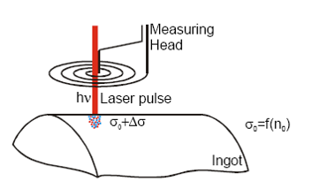
The e-PCD setup consists of a 980nm cw laser and an eddy current photoconductance sensor. This configuration ensures the deep carrier profile and deep sensed volume.
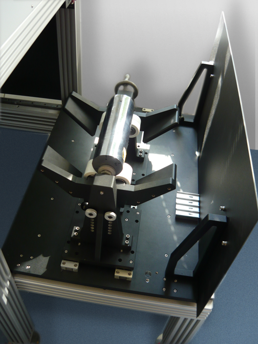
The system is able to record linescans along the ingots.
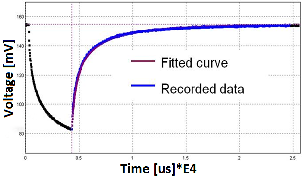
In the case of long carrier diffusion length, the shapes of the recorded transients are not exponential due to the recombination at the surface and due to the continuous in-diffusion of the carriers towards the bulk. Thus, the proper evaluation of the recorded PCD transients might be difficult.
A unique feature of Semilab's e-PCD technique is the transient evaluation routine. In spite of other techniques - applying complex calculations relying on various physical models, and material parameters input - the e-PCD algorythm is based on a mathematical-phenomenological transient curve fitting meghod. It provides a parameter-free, reliable and repeatable bulk lifetime determintaion of the actual sample.
FEATURES
- Bulk minority carrier measurement
- Deep penetration of excitation light and PCD sensing E-M field
- Excellent repeatability
- Unique – material parameter independent - evaluation method
- Bulk lifetime mapping
Product Line
WT
The WT product line is a powerful measurement platform for performing many different semiconductor material characterization measurements. The base system includes all the overhead functions necessary to perform characterization measurements, including power supplies, computer and operating software, XY measurement stage, etc. The WT-2000 is typically used to make maps, where the wafer is scanned at a programmable raster. Each system is configured to the user’s requirements by adding treatment and measurement capabilities.
Products

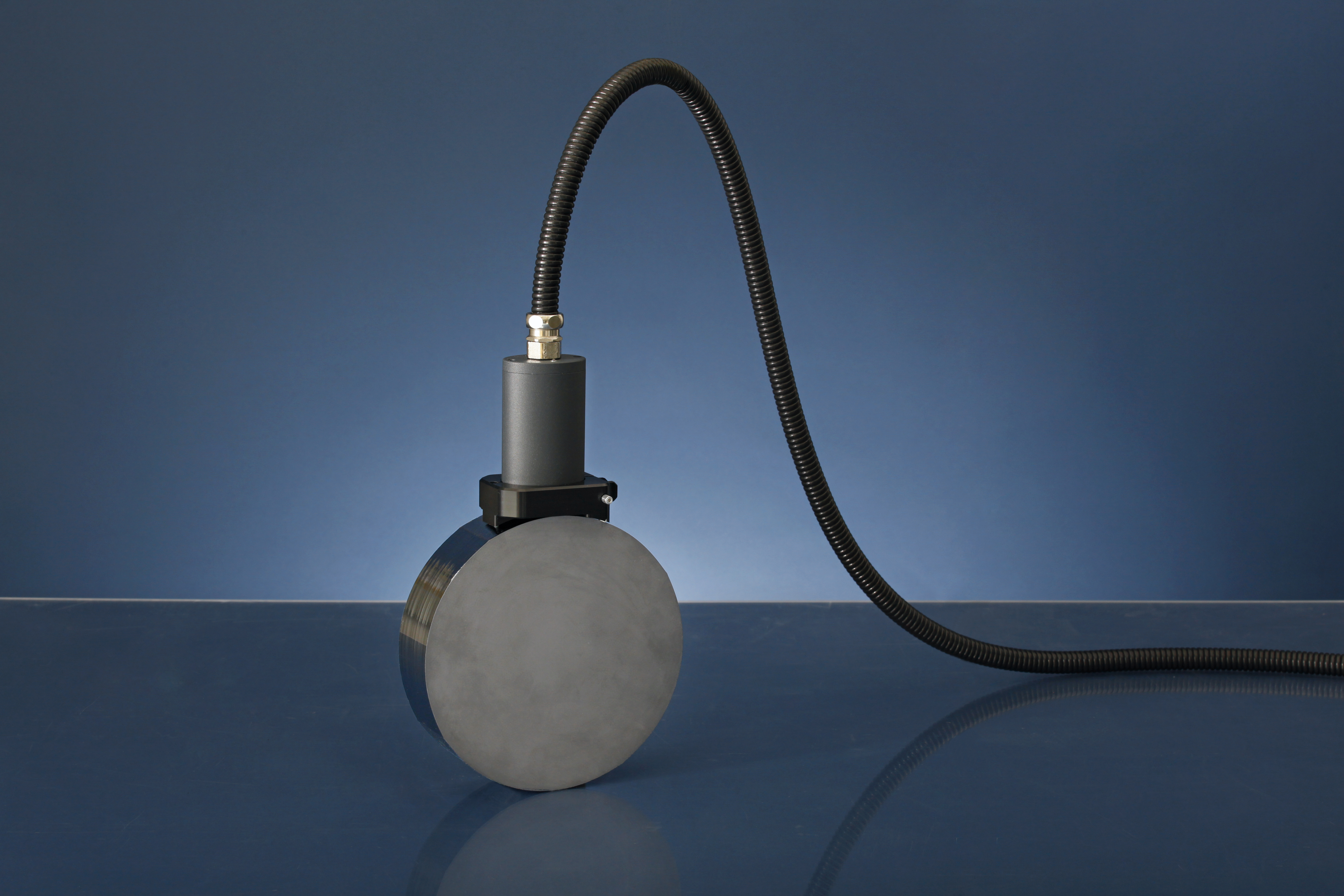
WT-1200iL
WT-1200iL is a non-contact hand-held tool for single point bulk lifetime measurements based on Eddy current detected photo conductance decay (e-PCD) specially for metal contamination detection of mono-crystalline ingots and slugs. It provides a good correlation with μ-PCD on surface passivated samples. The simple construction ensures the easy manageability.
Application:
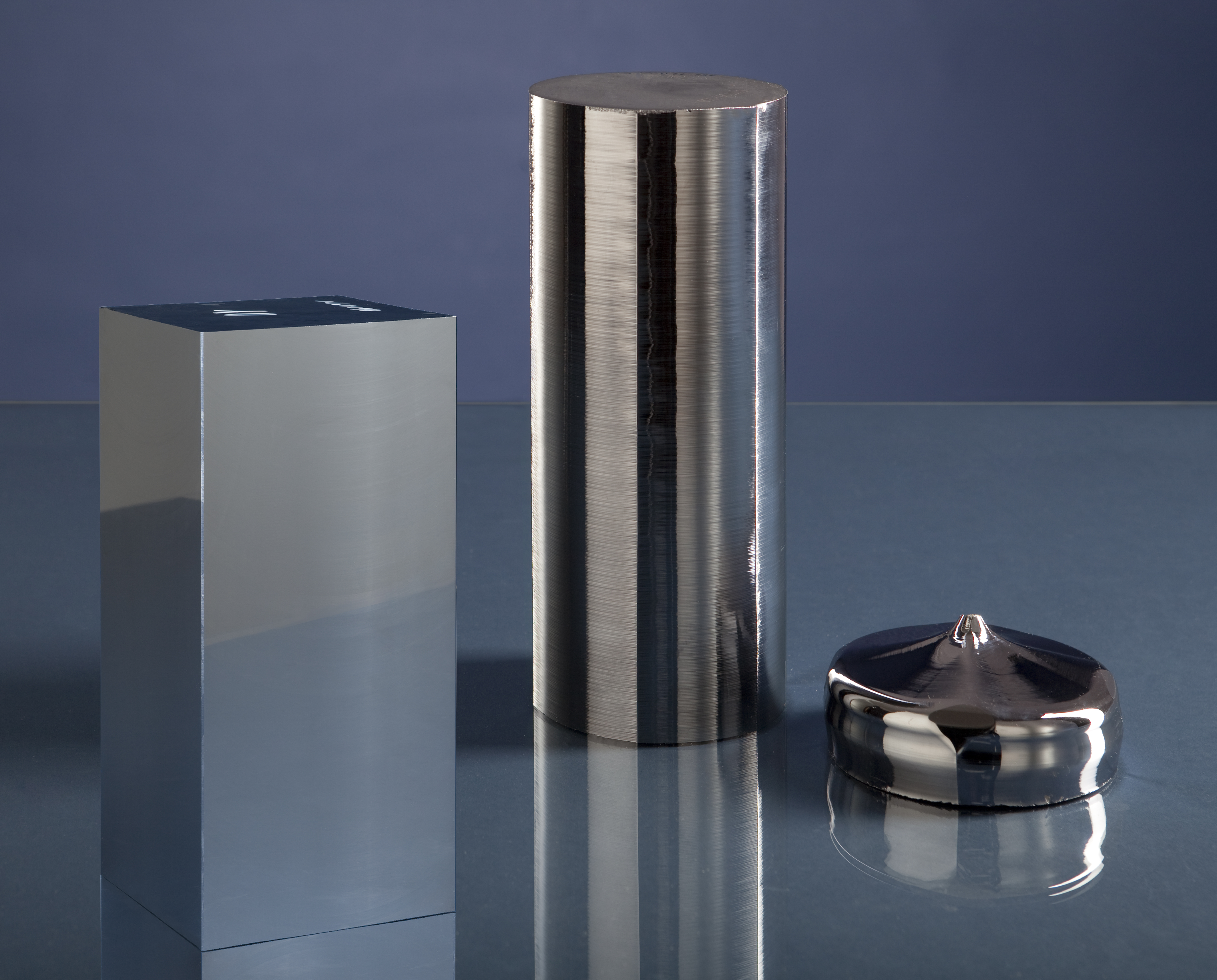
- Non-contact bulk lifetime and resistivity measurement on mono-crystalline ingots and slugs for process monitoring and feedstock characterization
- Suited for one-point measurement
- Bulk lifetime measurement without surface passivation and calibration
- Enables the bulk lifetime measurement at given injection levels (e.g. 1E15 1/cm3)
Options:
- Flexible platform for production line compatibility
- EDDY resistivity measuring
Software highlights:
- Easy exchange of data and images with other Windows applications
- Handling several data files at the same time
- Automatic data evaluation during measurement
- Open for local or remote database servers (ODBC)
- Open for communication like automatic or manual recording of ingot ID, light sensor signal acquisition